Semiconductor device

a technology of semiconductors and devices, applied in the direction of semiconductor devices, electrical equipment, transistors, etc., to achieve good electrical characteristics

Active Publication Date: 2012-01-05
SEMICON ENERGY LAB CO LTD
View PDF0 Cites 38 Cited by
  • Summary
  • Abstract
  • Description
  • Claims
  • Application Information

AI Technical Summary

Benefits of technology

[0025]According to one embodiment of the present invention, a semi...

Problems solved by technology

A transistor in which a channel region is formed in an oxide semiconductor has a problem: the threshold voltage (Vth) is easily shifted in the negative directi...

Method used


Image

  • Semiconductor device
  • Semiconductor device
  • Semiconductor device

Examples


embodiment 1

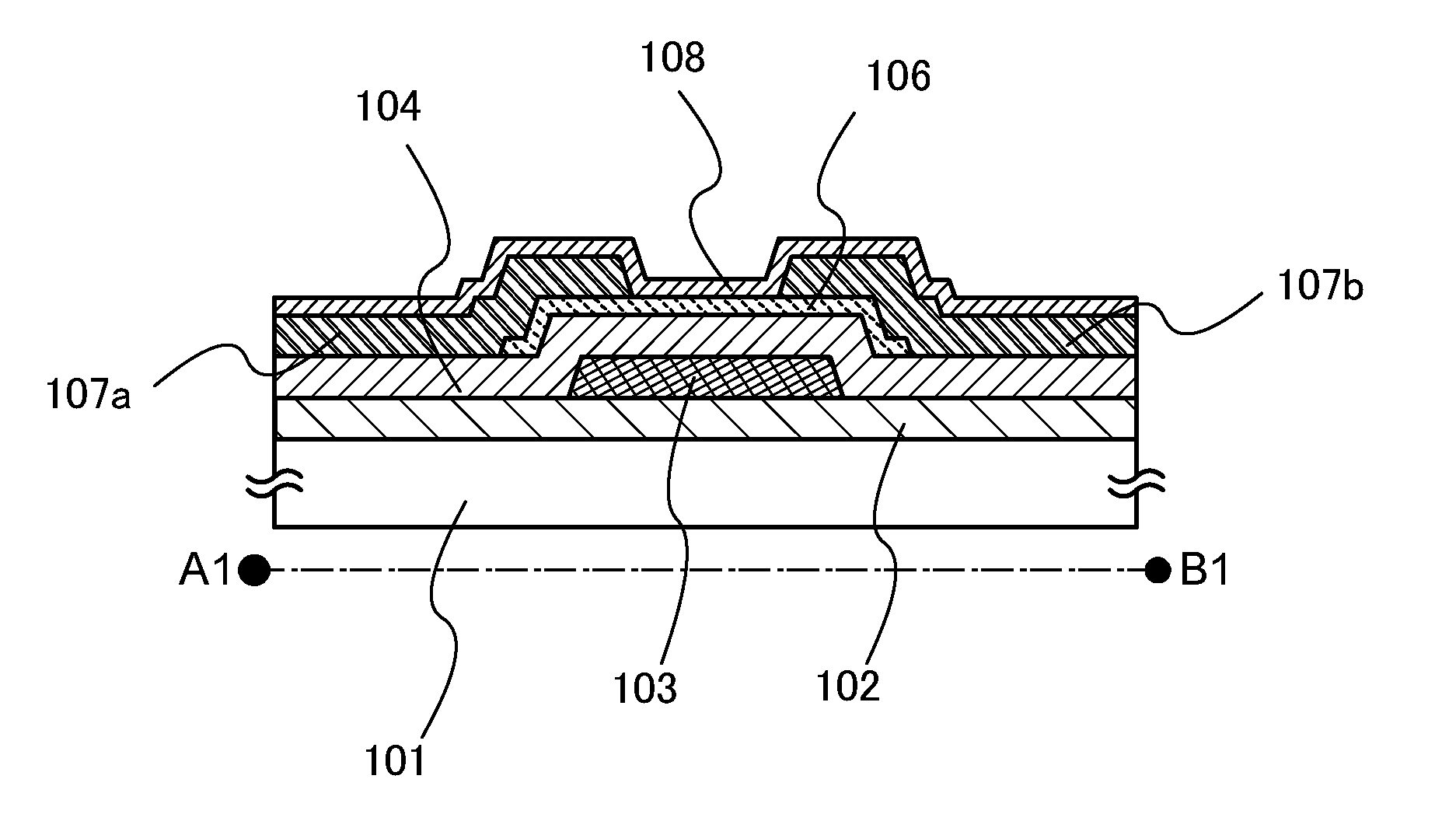
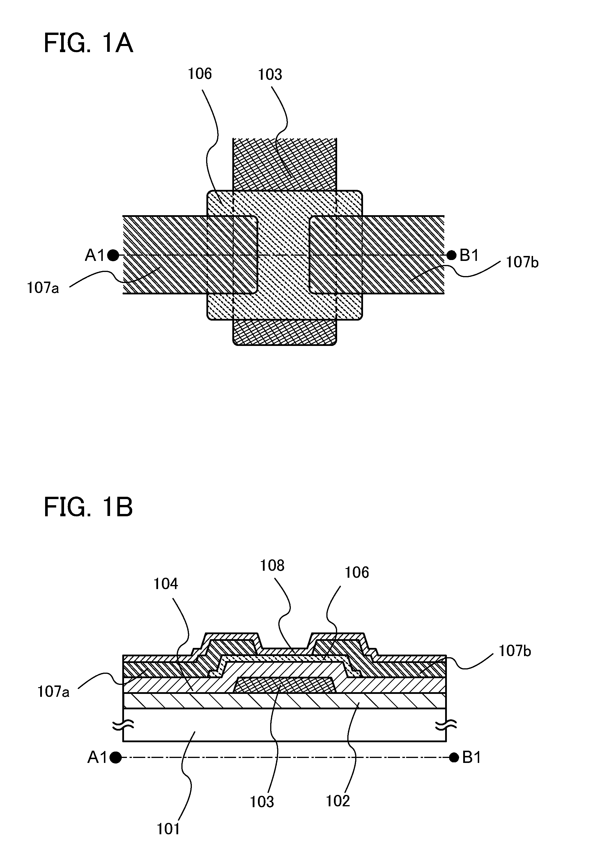
[0042]In this embodiment, a semiconductor device which is one embodiment of the present invention is described with reference to FIGS. 1A and 1B. Note that while a transistor is illustrated as an example of the semiconductor device in FIGS. 1A and 1B, one embodiment of the present invention can be similarly implemented using a diode and the like.

[0043]FIG. 1A is a top view of a transistor. FIG. 1B is a cross sectional view taken along line A1-B1 in FIG. 1A. The transistor includes, over a substrate 101, a base insulating layer 102, a gate electrode layer 103, a gate insulating layer 104, an oxide semiconductor layer 106 where a channel region is formed, a source electrode layer 107a and a drain electrode layer 107b, and an insulating layer 108 which covers the oxide semiconductor layer 106, the source electrode layer 107a, and the drain electrode layer 107b.

[0044]The transistor in FIGS. 1A and 1B is a transistor having a bottom-gate structure, in which the oxide semiconductor layer...

embodiment 2

[0123]In this embodiment, an example where a silicon oxide layer with a low hydrogen concentration is used as a base insulating layer of a top-gate transistor will be described with reference to FIGS. 7A to 7C. The silicon oxide layer is formed by a plasma CVD method using silicon tetrafluoride which is a deposition gas, nitrous oxide which is an oxidizing gas, and argon which stably generates plasma.

[0124]A base insulating layer 202 including silicon oxide as its main component is formed over the substrate 201. As described above, the base insulating layer 202 is formed by a plasma CVD method using silicon tetrafluoride. For details of the formation method, a manufacturing method of the gate insulating layer 104 in Embodiment 1 may be referred to. The thickness of the base insulating layer 202 is preferably five or more times as thick as the total thickness of an oxide semiconductor layer and a gate insulating layer which are formed later.

[0125]When the base insulating layer 202 ha...

embodiment 3

[0139]In this embodiment, an example where a silicon oxide layer with a low hydrogen concentration which is formed by using silicon tetrafluoride as a deposition gas is used as a base insulating layer of a top-gate transistor will be described with reference to FIGS. 8A to 8D.

[0140]A base insulating layer 302 including silicon oxide as its main component is formed over the substrate 301. As described above, the base insulating layer 302 is formed by a plasma CVD method using silicon tetrafluoride. For details of the formation method, a manufacturing method of the gate insulating layer 104 in Embodiment 1 may be referred to. The thickness of the base insulating layer 302 is preferably five or more times as thick as the total thickness of an oxide semiconductor layer and a gate insulating layer which are formed later.

[0141]After that, an In—Ga—Zn—O-based film with a thickness of 10 nm to 30 nm is formed by a sputtering method as an oxide semiconductor film 303. Then, a conductive film...


PUM


Abstract

In a transistor including an oxide semiconductor, hydrogen in the oxide semiconductor leads to degradation of electric characteristics of the transistor. Thus, an object is to provide a semiconductor device having good electrical characteristics. An insulating layer in contact with an oxide semiconductor layer where a channel region is formed is formed by a plasma CVD method using a silicon halide. The insulating layer thus formed has a hydrogen concentration less than 6×10²⁰ atoms/cm3 and a halogen concentration greater than or equal to 1×10²⁰ atoms/cm3; accordingly, hydrogen diffusion into the oxide semiconductor layer can be prevented and hydrogen in the oxide semiconductor layer is inactivated or released from the oxide semiconductor layer by the halogen, whereby a semiconductor device having good electrical characteristics can be provided.

Description

BACKGROUND OF THE INVENTION[0001]1. Field of the Invention[0002]One embodiment of the present invention relates to a semiconductor device including an oxide semiconductor and a manufacturing method thereof.[0003]In this specification, the term semiconductor device refers to all devices that can function by utilizing semiconductor characteristics, and electrooptic devices, semiconductor circuits, and electronic devices are all semiconductor devices.[0004]2. Description of the Related Art[0005]In recent years, transistors are used for many liquid crystal display devices and light-emitting display devices typified by flat panel displays, and they are formed with silicon semiconductors, such as amorphous silicon or polycrystalline silicon, over a glass substrate.[0006]Attention has been directed to a technique in which, instead of such silicon semiconductors, oxide semiconductors are used for transistors.[0007]Examples of the oxide semiconductor include zinc oxide, which is one-metal ox...

Claims


Application Information

Patent Timeline
IPC IPC(8): H01L29/786
CPCH01L29/7869H01L29/78606H01L29/4908H01L29/51
Inventor ICHIJO, MITSUHIROENDO, TOSHIYASUZUKI, KUNIHIKOTAKEMURA, YASUHIKO
Owner SEMICON ENERGY LAB CO LTD
Why Eureka
Try Eureka