SiC semiconductor device and method for manufacturing the same

a semiconductor device and semiconductor technology, applied in the direction of semiconductor devices, basic electric elements, electrical appliances, etc., can solve the problems of inability to thicken by thermal oxidation, inability to use mos interface formation method, and time-consuming mos polishing for processing substrate surfaces using oxidation reactions, etc., to achieve high channel mobility and reduce interface state density. , the effect of low density

Active Publication Date: 2008-08-28
DENSO CORP
View PDF18 Cites 36 Cited by
  • Summary
  • Abstract
  • Description
  • Claims
  • Application Information

AI Technical Summary

Benefits of technology

[0011]By maintaining the wet atmosphere or the hydrogen atmosphere continuously in the reducing the temperature, the dangling bond at an interface between the gate insulating film and the channel region is terminated with the H atom or the OH group. Thus, the interface state density lowers and a silicon carbide semiconductor device with a high channel mobility can be provided.

Problems solved by technology

Therefore, the wafer with the (0001) Si face has the problems that it cannot be thickened by thermal oxidation and that CMP polishing for processing the substrate surface using an oxidation reaction takes a time.
However, a MOS interface formation method which reduces the interface state density at the (000-1) C face has not been disclosed.

Method used


Image

  • SiC semiconductor device and method for manufacturing the same
  • SiC semiconductor device and method for manufacturing the same
  • SiC semiconductor device and method for manufacturing the same

Examples


first embodiment

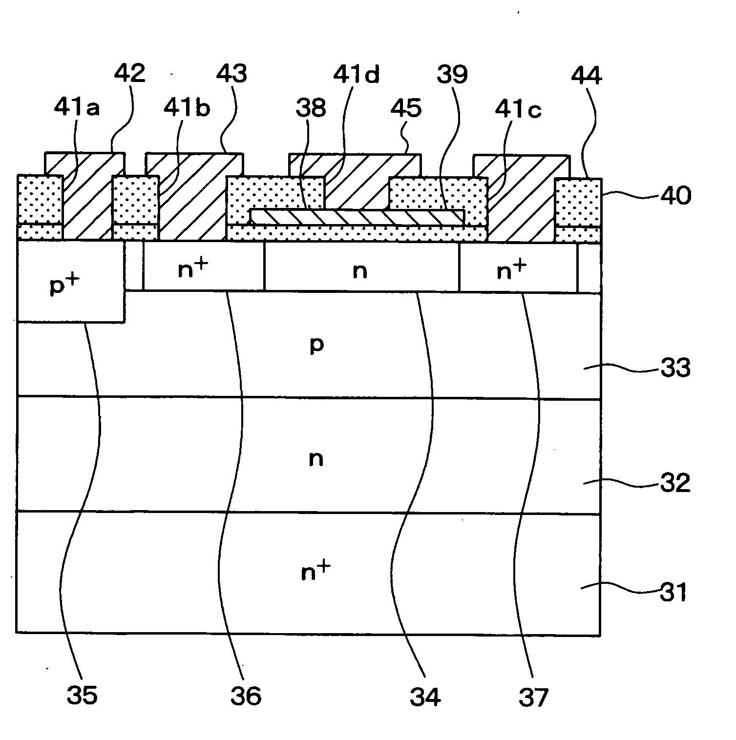
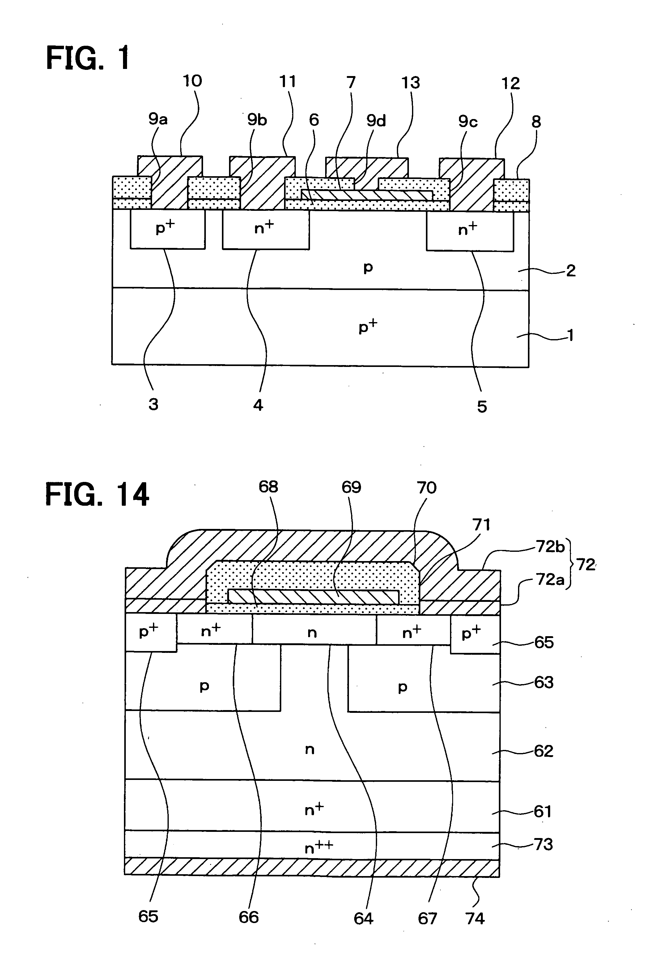
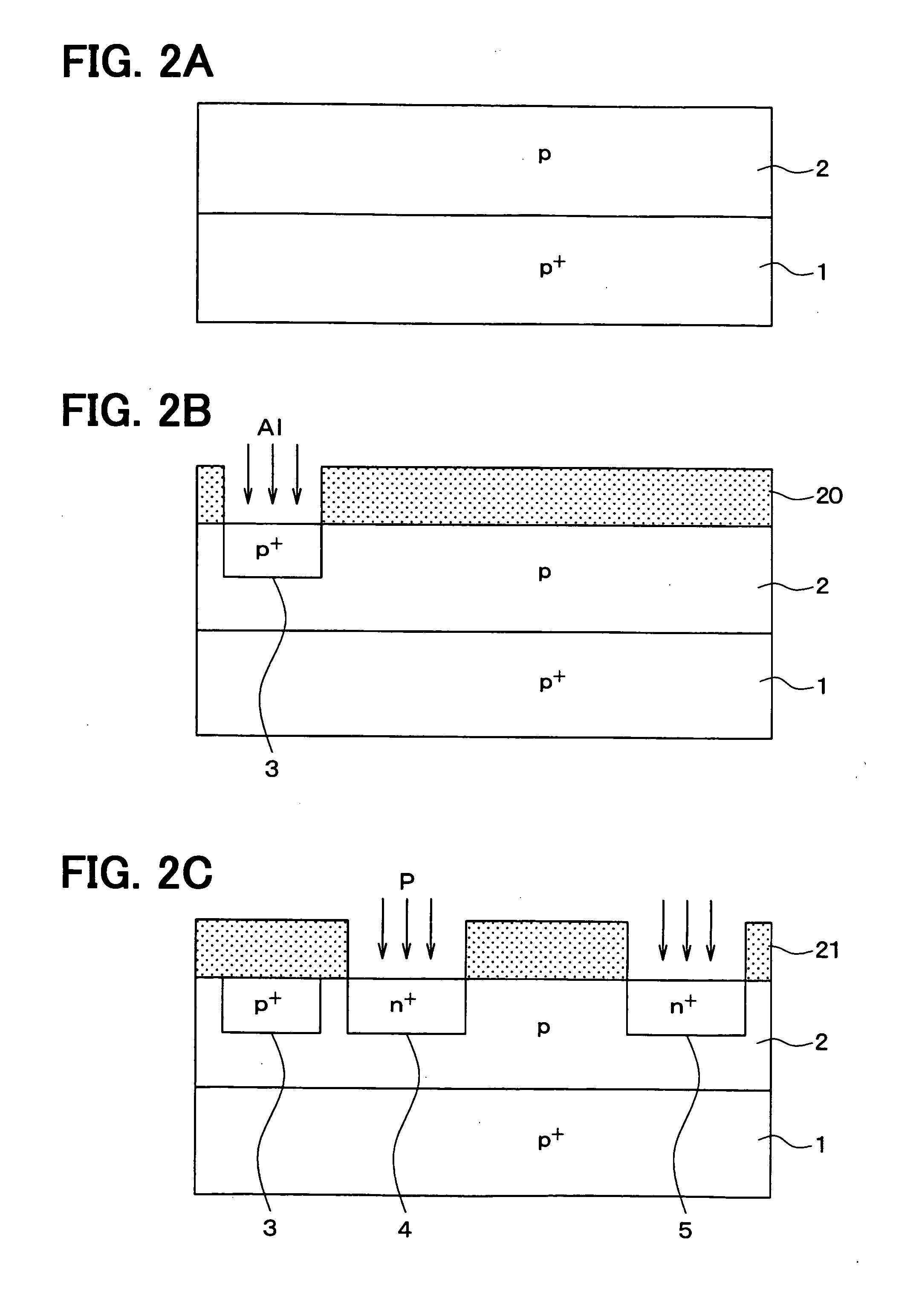
[0065]In view of the above study, in the present embodiment, an inversion-mode lateral MOSFET is provided. FIG. 1 shows a cross-sectional structure of the inversion-mode lateral MOSFET, while FIGS. 2A to 2C and 3A to 3C show the steps of manufacturing the inversion-mode lateral MOSFET shown in FIG. 1. Referring to these drawings, the structure and manufacturing method of the inversion-mode lateral MOSFET according to the present embodiment will be described.

[0066]As shown in FIG. 1, a p+-type substrate 1 made of SiC has a principal surface on one side thereof, and a p-type base layer 2 made of epitaxially grown SiC is formed on the principal surface of the p+-type substrate 1 to provide a p / p+ substrate used as a semiconductor substrate. As the p+-type substrate 1, a substrate made of, e.g., 4H—SiC, having a (000-1) C face as the principal surface, and having an impurity concentration of about 5×1018 cm−3 is used. The p-type base layer 2 has an impurity concentration of, e.g., about...

second embodiment

[0087]The present embodiment also relates to the inversion-mode lateral MOSFET. The present embodiment is different from the first embodiment in that the method of manufacturing the inversion-mode lateral MOSFET is partly changed, and is the same as the first embodiment in terms of the structure of the inversion-mode lateral MOSFET and the like.

[0088]The inversion-mode lateral MOSFET according to the present embodiment is manufactured by adding the manufacturing step shown in FIG. 6 to the method of manufacturing the inversion-mode lateral MOSFET shown in FIGS. 2A to 2C and 3A to 3C according to the first embodiment.

[0089]That is, after performing the individual steps shown in FIGS. 2A to 2C and FIGS. 3A and 3B, the process shown in FIG. 6 is performed. Thereafter, by performing the process shown in FIG. 3C and the like, the inversion-mode lateral MOSFET having the same structure as in the first embodiment is manufactured.

[0090]Specifically, in the step shown in FIG. 6, round-off ox...

third embodiment

[0095]The present embodiment also relates to the inversion-mode lateral MOSFET. The present embodiment is different from the first or second embodiment in that the method of manufacturing the inversion-mode lateral MOSFET is partly changed, and is the same as the first or second embodiment in terms of the structure of the inversion-mode lateral MOSFET and the like.

[0096]The inversion-mode lateral MOSFET according to the present embodiment is manufactured by changing the step of forming the interlayer insulating film 8 shown in FIG. 3C of the method of manufacturing the inversion-mode lateral MOSFET shown in FIGS. 2A to 2C and 3A to 3C (and FIG. 6) described above to the step shown in FIGS. 8A and 8B.

[0097]That is, by performing the individual steps shown in FIGS. 2A to 2C and FIGS. 3A and 3B (or further performing the process shown in FIG. 6) and subsequently performing the process shown in FIGS. 8A and 8B, instead of the process shown in FIG. 3C, the inversion-mode lateral MOSFET h...


PUM


Abstract

A SiC semiconductor device having a MOS structure includes: a SiC substrate; a channel region providing a current path; first and second impurity regions on upstream and downstream sides of the current path, respectively; and a gate on the channel region through the gate insulating film. The channel region for flowing current between the first and second impurity regions is controlled by a voltage applied to the gate. An interface between the channel region and the gate insulating film has a hydrogen concentration equal to or greater than 4.7×1020 cm−3. The interface provides a channel surface having a (000-1)-orientation surface.

Description

CROSS REFERENCE TO RELATED APPLICATION[0001]This application is based on Japanese Patent Application No. 2007-49705 filed on Feb. 28, 2007, the disclosure of which is incorporated herein by reference. This application is also related to U.S. application Ser. No. ______, entitled “SIC SEMICONDUCTOR DEVICE AND METHOD FOR MANUFACTURING THE SAME”, filed on ______.FIELD OF THE INVENTION[0002]The present invention relates to a SiC semiconductor device and a method for manufacturing a SiC semiconductor device.BACKGROUND OF THE INVENTION[0003]Japanese Patent Application Laid-Open Publication No. 2003-69012 corresponding to U.S. Pat. No. 6,764,963 discloses a conventional method which performs treatment with hydrogen annealing or a wet atmosphere in a SiC semiconductor device using a crystal a-face with a (11-20) face orientation for a channel, thereby reducing an interface state density in a MOS structure and improving a channel mobility. Specifically, the reduction in interface state densi...

Claims


Application Information

Patent Timeline
Patent Type & Authority Applications(United States)
IPC IPC(8): H01L29/772H01L21/04
CPCH01L21/049H01L29/045H01L29/0847H01L29/1083H01L29/1087Y10S438/931H01L29/51H01L29/66068H01L29/78H01L29/7828H01L29/7838H01L29/1608
Inventor ENDO, TAKESHI
Owner DENSO CORP
Why Eureka
Try Eureka