Semiconductor structure and fabricating method thereof

a technology of semiconductors and structures, applied in semiconductor devices, semiconductor/solid-state device details, electrical devices, etc., can solve the problems of the most serious damage at the cross of the scribe line, the material layer disposed on the scribe line may be damaged or cracked, and the complex fabrication process of the integrated circuit devi

Active Publication Date: 2007-03-29
MARLIN SEMICON LTD
View PDF7 Cites 16 Cited by
  • Summary
  • Abstract
  • Description
  • Claims
  • Application Information

AI Technical Summary

Benefits of technology

[0008] Accordingly, the present invention is directed to provide a semiconductor structure, which can prevent the corners of the chips from cracking when the chip is scribed.
[0009] Another objective of the present invention is to provide a fabricating method of the semiconductor structure to prevent the corners of the chips from cracking by forming a metal pattern in the dielectric layer and surrounding the chip area of the wafer.
[0024] As a plurality of metal patterns is formed in each dielectric layer around the chips, when the chip is being scribed, the metal patterns can avoid the formation of cracks between the layers or especially at the corners of the chip. Therefore, the performance and reliability of the devices are improved. In addition, no extra step is required for the fabrication.

Problems solved by technology

However, the fabrication processes of integrate circuit devices are very complicated, basically including four main stages: integrate circuit design, wafer fabrication, wafer testing and wafer packaging.
Since material layers of different materials are formed covering the wafer, the material layers disposed on the scribe line may be damaged or cracked when the wafer is scribed.
Particularly, the above damages are near the corners of the chip.
That is, the damages at the crosses of the scribe lines are the most serious because the stress focuses on the crosses of the scribe lines.
Moreover, even after packaging, the external influences, i.e., the temperature changes, may result in the extension of cracks or delamination.
It is because the adhesion between the low-k dielectric material layer and other dielectric layers or metal layers is usually not good.
Accordingly, the performance of the device may be degraded or the lifetime may be reduced, thus increasing the costs of packaging processes and lowering the reliability of devices.

Method used


Image

  • Semiconductor structure and fabricating method thereof
  • Semiconductor structure and fabricating method thereof
  • Semiconductor structure and fabricating method thereof

Examples


Embodiment Construction

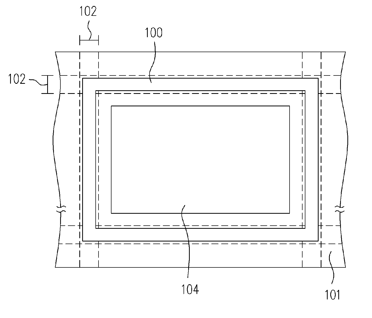
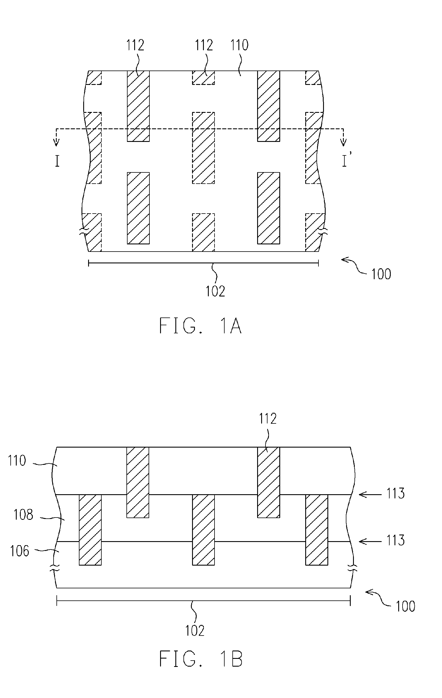
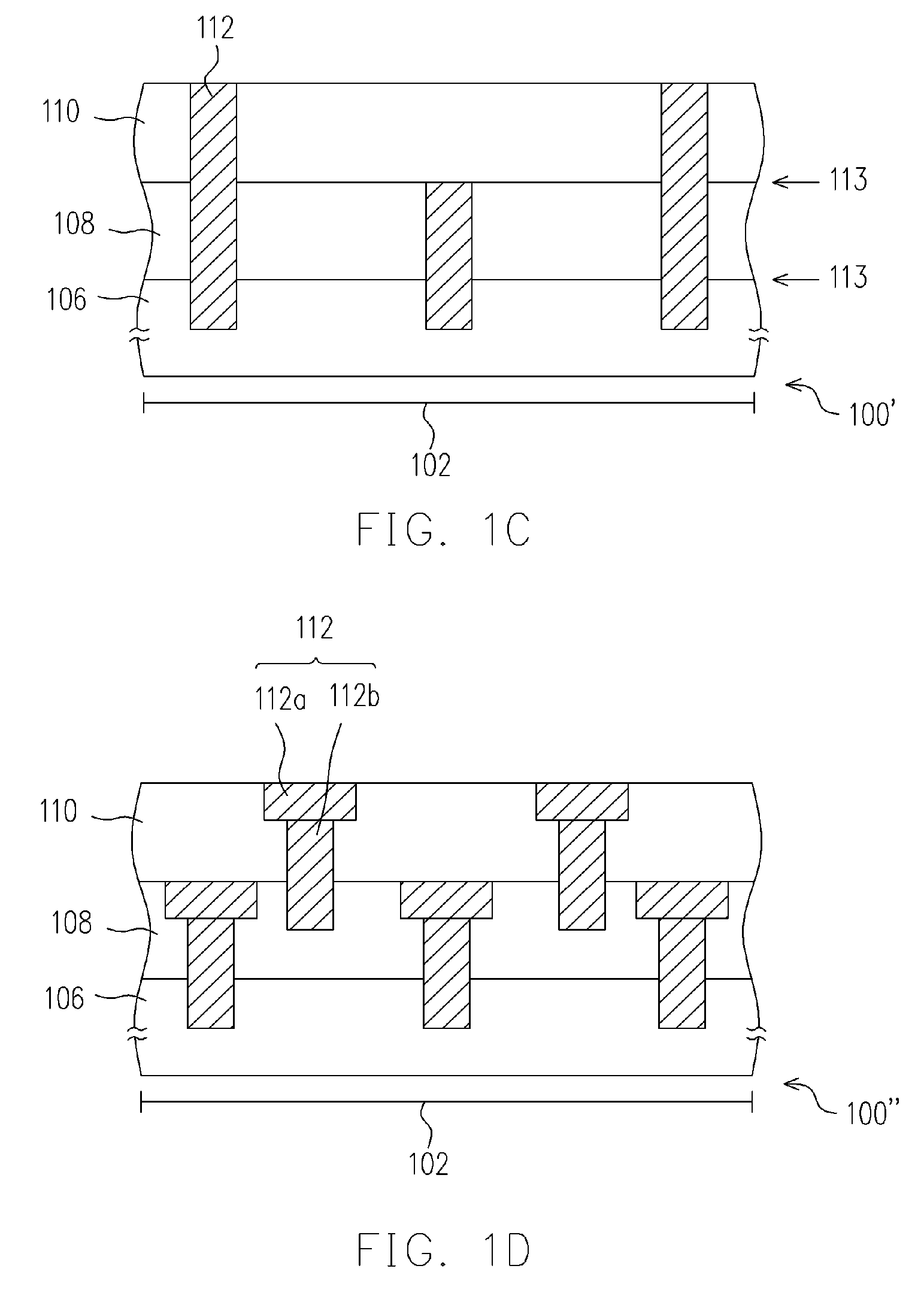
[0034]FIG. 1A is a top view of the semiconductor structure according to one embodiment of the present invention. FIG. 1B is a cross-sectional view of a semiconductor structure along line I-I as shown in FIG. 1A. FIG. 1C is a schematic cross-sectional view of a semiconductor structure according to another embodiment of the present invention. FIG. 1D is a schematic cross-sectional view of a semiconductor structure according to another embodiment of the present invention. FIG. 2 is a top view of the semiconductor structure and the chip area according to the embodiment of the present invention.

[0035] Referring to FIG. 1A, FIG. 1B and FIG. 2 simultaneously, the semiconductor structure 100 is disposed on the scribe lines 102 of a wafer 101 and surrounding the chip area 104 of the wafer 101, wherein the chip area 104 has, for example, a MOS transistor, other semiconductor devices or circuits. The semiconductor structure 100 includes dielectric layers 106, 108, 110 and metal patterns 112. ...


PUM


Abstract

A semiconductor structure is provided. The semiconductor structure is disposed on the scribe line of a wafer and is around the chip area of the wafer. The semiconductor structure includes a plurality of dielectric layers sequentially disposed on the scribe line and a plurality of metal patterns disposed in each dielectric layer. The metal patterns disposed in each dielectric layer extend to the next underlying dielectric layer.

Description

BACKGROUND OF THE INVENTION [0001] 1. Field of Invention [0002] The present invention relates to a semiconductor structure and a fabricating method thereof. More particularly, the present invention relates to a semiconductor structure and a fabricating method thereof, which prevents the chip from cracking. [0003] 2. Description of Related Art [0004] The integrate circuit (IC) devices have almost been applied everywhere along with the quick developments of the semiconductor manufacture. However, the fabrication processes of integrate circuit devices are very complicated, basically including four main stages: integrate circuit design, wafer fabrication, wafer testing and wafer packaging. In general, about hundreds of different process steps are required for the fabrication of the IC devices and the whole procedure may need one or two months to complete. [0005] In order to achieve mass production and cost reduction, the diameter of the wafer has been evolved to 12 inches from the early...

Claims


Application Information

Patent Timeline
Patent Type & Authority Applications(United States)
IPC IPC(8): H01L23/544H01L21/30
CPCH01L23/5283H01L23/53295H01L23/585H01L2924/0002H01L2924/00
Inventor KUO, CHIEN-LIWU, BING-CHANGJAO, JUI-MENG
Owner MARLIN SEMICON LTD
Why Eureka
Try Eureka