Blue organic electroluminescent device
- Summary
- Abstract
- Description
- Claims
- Application Information
AI Technical Summary
Benefits of technology
Problems solved by technology
Method used
Image

Examples
example 1
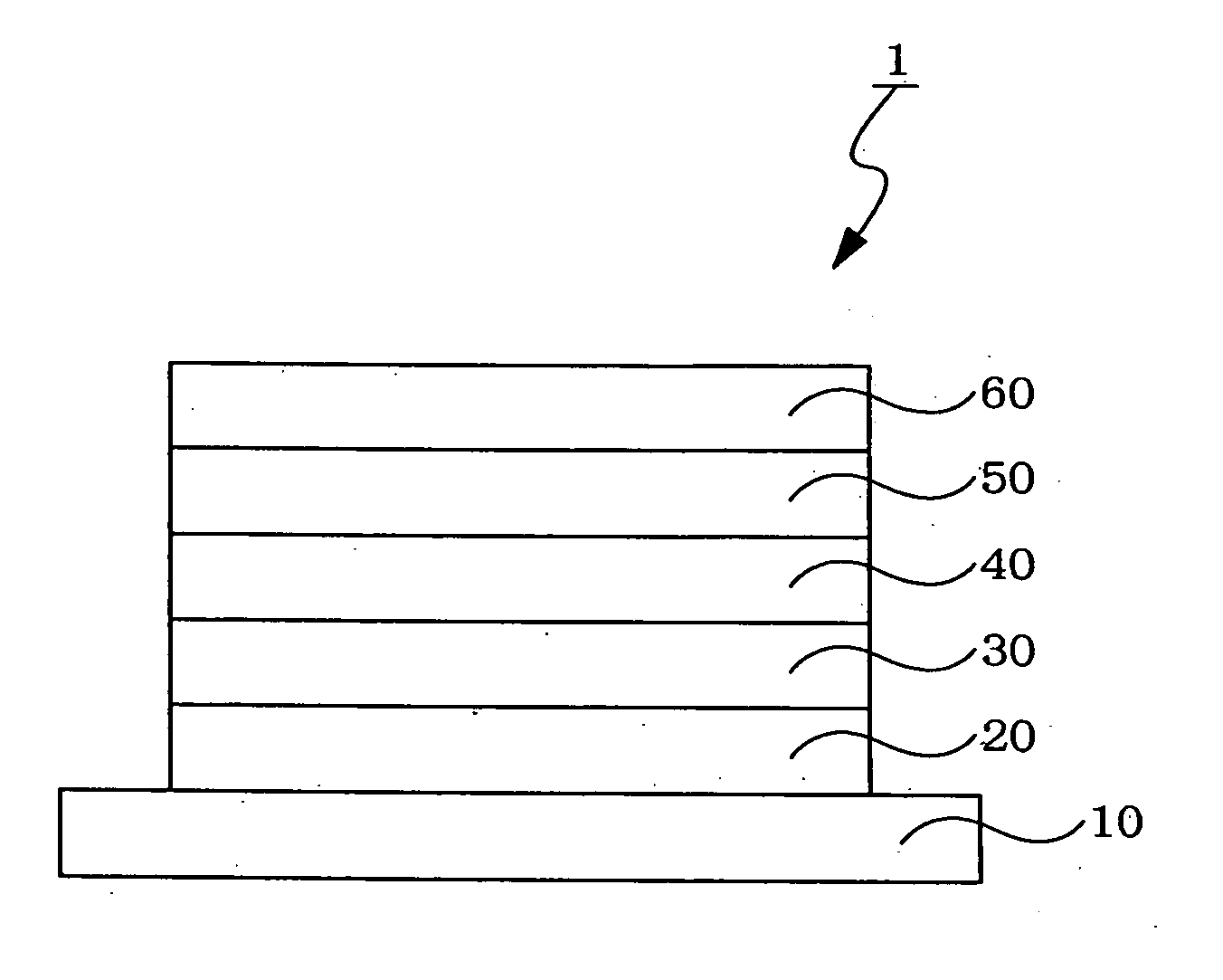
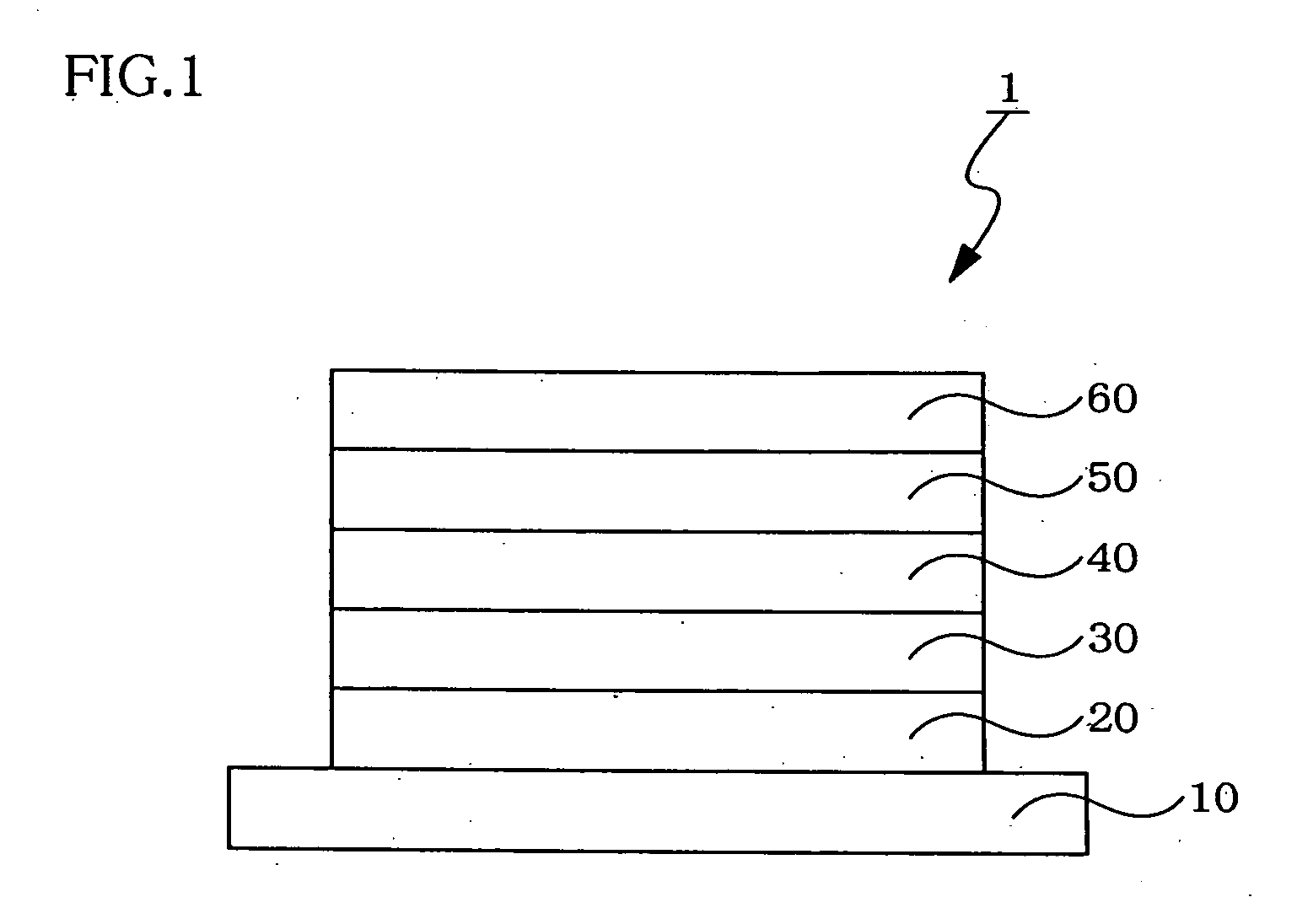
[0125] A glass substrate (25×75×1.1 mm, manufactured by Geomatics) provided with an ITO transparent electrode was subjected to ultrasonic cleaning for five minutes in isopropyl alcohol and then subjected to UV ozone cleaning for 30 minutes. The cleaned glass substrate with the linear transparent electrode was installed in a substrate holder of a vacuum deposition device, and an HIM (Egs=3.3 eV, EgT=2.5 eV) film with a thickness of 40 nm was formed by resistance heating deposition on the surface of the glass substrate on which the linear transparent electrode was formed so that the transparent electrode was covered. The HIM film functioned as a hole transporting layer (hole injecting layer). A TCTA(Egs=3.3 eV, EgT=3.0 eV) film (hole transporting layer) with a thickness of 40 nm was formed on the HIM film by resistance heating deposition.
[0126] As a host compound, the compound (A) (Ip=6.0 eV, Egs=3.4 eV, EgT=2.9 eV, Af=2.6 eV) was deposited on the TCTA film to a thickness of 20 nm to...
example 2
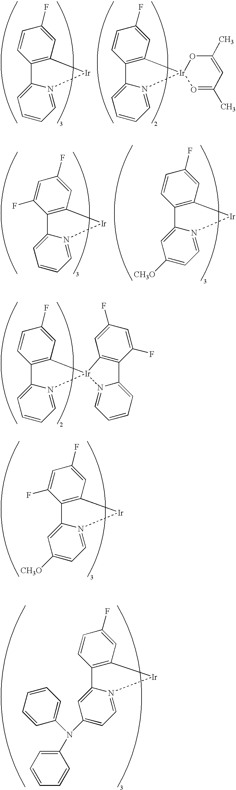
[0130] A device was fabricated in the same manner as in Example 1 except for using the compound (B2) (peak wavelength in the ultraviolet luminescence region: 400 nm, Ip=5.1 eV, Egs=3.54 eV (absorption edge), EgT=3.3 eV, Af=1.56 eV) as the ultraviolet luminescent dopant instead of the compound (B1).
[0131] After sealing the resulting device, electricity was supplied to the device for test. Blue green light with a luminance of 105 cd / m2 was obtained at a voltage of 7.0 V and a current density of 0.35 mA / cm2. The luminous efficiency was 30 cd / A.
[0132] The device was caused to emit light at a luminance of 100 cd / m2, and the EL spectrum was measured. The peak wavelength was 486 nm. Since the luminous intensity (emission wavelength peak (400 nm)) of the complex (B2) in the EL spectrum was zero, the intensity ratio was zero.
PUM
| Property | Measurement | Unit |
|---|---|---|
| Nanoscale particle size | aaaaa | aaaaa |
| Energy gap | aaaaa | aaaaa |
| Electron affinity | aaaaa | aaaaa |
Abstract
Description
Claims
Application Information
 - Generate Ideas
- Intellectual Property
- Life Sciences
- Materials
- Tech Scout
- Unparalleled Data Quality
- Higher Quality Content
- 60% Fewer Hallucinations
Browse by: Latest US Patents, China's latest patents, Technical Efficacy Thesaurus, Application Domain, Technology Topic, Popular Technical Reports.
© 2025 PatSnap. All rights reserved.Legal|Privacy policy|Modern Slavery Act Transparency Statement|Sitemap|About US| Contact US: help@patsnap.com