Multi-port semiconductor memory device

Active Publication Date: 2007-03-29
SK HYNIX INC
View PDF18 Cites 29 Cited by
  • Summary
  • Abstract
  • Description
  • Claims
  • Application Information

AI Technical Summary

Benefits of technology

[0020] Embodiments of the present invention are directed to a semiconductor memory device for reliably performing a data communication with external devices through a plurality of ports.
[0021] In accordance with an aspect of the present invention, there is provided a semiconductor memory device including: a plurality of ports, a plurality of banks, a global data bus, a test mode determiner, a test input/output (I/O) controller; and a plurality of selectors. The ports perform a serial I/O data communication with external devices. The banks perform a parallel I/O data communication with the ports. The global data bus transmits a signal between the banks and the ports. The test mode determiner determines an operation mode of the semiconductor memory device by generating a test mode enable signal in response to a test mode control signal. The test I/O controller transmits and receives a test signal with the ports in response to the test mode enable signal during a port test mode. Each of the selectors receives the test signal output from the corresponding port in series and feedback the test signal to the corresponding port. The operation mode includes the port test mode for testing an operation of the ports and a normal operation mode for da

Problems solved by technology

However, because a large number of buses are included for the parallel I/O interface, a dat

Method used


Image

  • Multi-port semiconductor memory device
  • Multi-port semiconductor memory device
  • Multi-port semiconductor memory device

Examples


Embodiment Construction

[0037] Hereinafter, a delay locked loop (DLL) device in accordance with the present invention will be described in detail referring to the accompanying drawings.

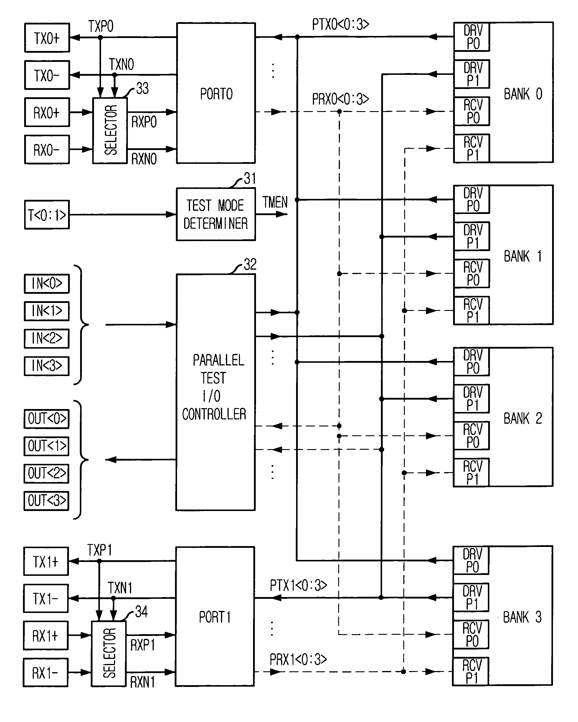
[0038]FIG. 3 is a block diagram of the semiconductor memory device in accordance with an embodiment of the present invention.

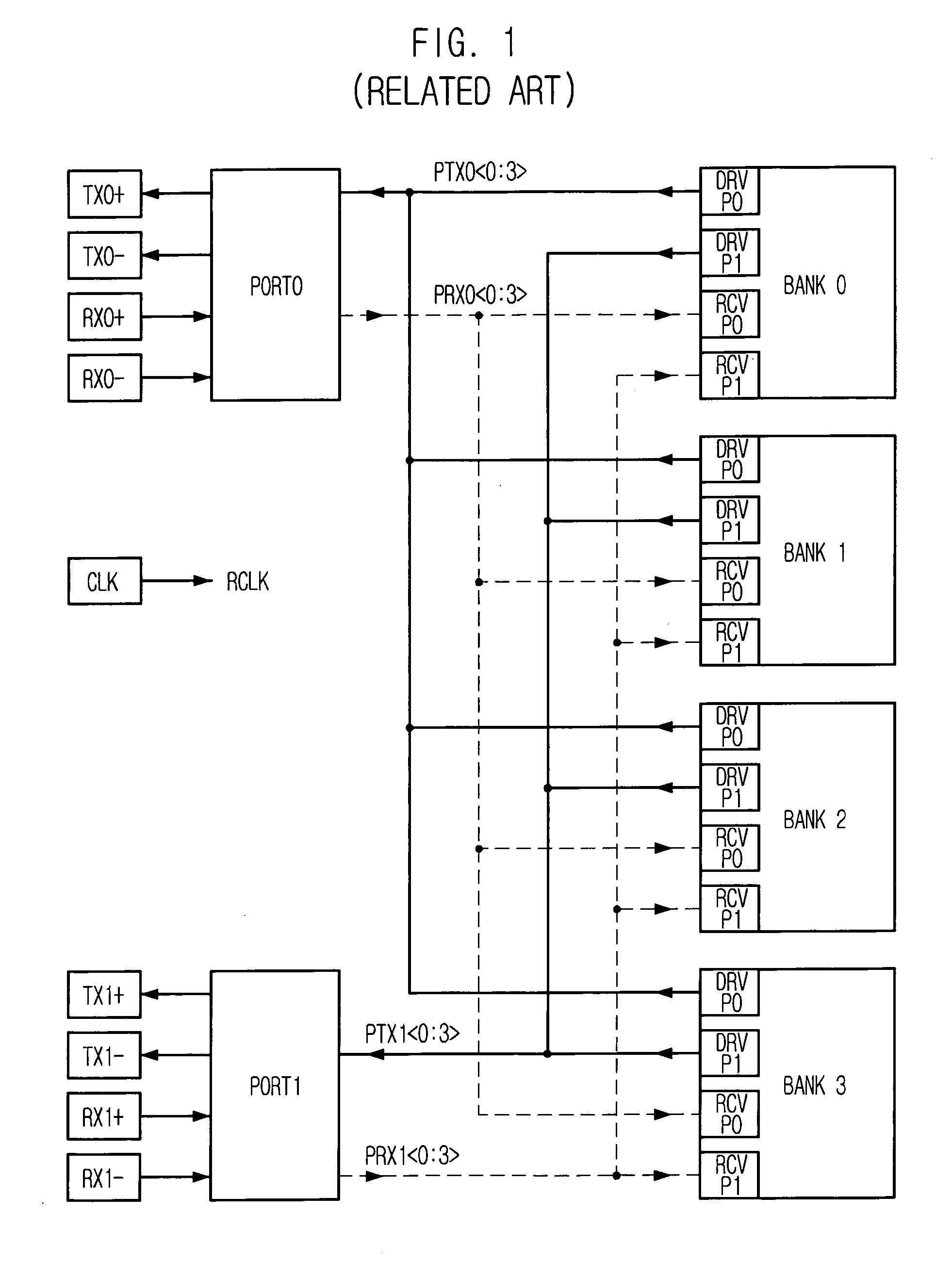
[0039] As shown, the semiconductor memory device includes two ports PORT0 and PORT1, four banks BANK0 to BANK3, a plurality of serial input / output (I / O) pads TX0+, TX0−, RX0+, RX0−, TX1+, TX1−, RX1+, and RX1−, a plurality of parallel I / O pads IN0:3>, T0:1>, and OUT0:3>. The semiconductor memory device further includes a test mode determiner 31 and a parallel test I / O controller 32.

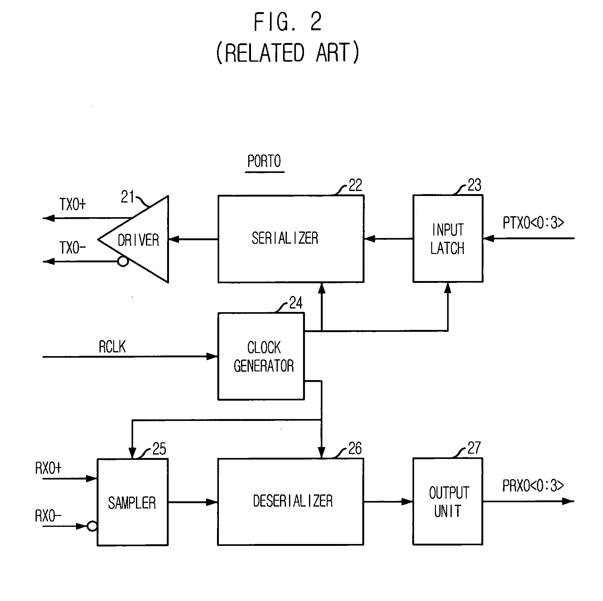
[0040] The serial I / O pads TX0+, TX0−, RX0+, RX0−, TX1+, TX1−, RX1+, and RX1− are used for communication between external devices and the ports PORT0 and PORT1 at a high speed. The serial I / O pads includes serial transmission I / O pads TX0+, TX0−, TX1+ and TX1− for transmitting a serial output data signal output from the po...


PUM


Abstract

A semiconductor memory device includes: a plurality of ports configured to perform a serial input/output (I/O) data communication with external devices; a plurality of banks configured to perform a parallel I/O data communication with the ports; a global data bus configured to transmit a signal between the banks and the ports; a test mode determiner configured to determine an operation mode of the semiconductor memory device by generating a test mode enable signal in response to a test mode control signal; a test I/O controller configured to transmit and receive a test signal with the ports in response to the test mode enable signal during a port test mode; and a plurality of selectors, each of which is configured to receive the test signal output from the corresponding port in series and feedback the test signal to the corresponding port.

Description

FIELD OF THE INVENTION [0001] The present invention relates to a semiconductor memory device, and more particularly to a semiconductor memory device including a plurality of ports for transmitting information with external devices. DESCRIPTION OF RELATED ARTS [0002] Most memory devices such as a random access memory (RAM) include only one port for transmitting data with external chipsets. The port is constituted with a plurality of input / output (I / O) pins. The memory device including single port employs a parallel I / O interface for concurrently transmitting multi-bit data through a plurality of data lines connected to the plurality of I / O pins respectively. The I / O interface uses a data transmission scheme for transmitting data via data lines, each of which is connected between two devices. The data line uses a bus for transmitting signals such as an address signal, a data signal, and a control signal. [0003] The parallel I / O interface provides a high data process speed because it c...

Claims


Application Information

Patent Timeline
IPC IPC(8): G11C29/00
CPCG11C29/26G11C8/16G11C29/1201G11C29/14G11C2207/105
Inventor DO, CHANG-HOLEE, JAE-JIN
Owner SK HYNIX INC
Why Eureka
Try Eureka