Semiconductor failure analysis tool

a technology of failure analysis and semiconductors, applied in semiconductor/solid-state device testing/measurement, manufacturing tools, instruments, etc., can solve the problems of inability to precisely target individual circuit elements, process does not lend itself to opening up regions of irregular shape, and the difficulty of isolating and analysing defects has become a greater challeng

Inactive Publication Date: 2007-04-05
CONTROLLED SEMICON
View PDF14 Cites 45 Cited by
  • Summary
  • Abstract
  • Description
  • Claims
  • Application Information

AI Technical Summary

Benefits of technology

[0010] Another method of removing material in a decapsulation process includes performing a sequence of steps, including two or more laser ablation steps performed along scan paths, on a packaged electronic device of the type encapsulated with a protective material that forms an outer surface of the device, in which material of a first layer is removed from a region of the device until a final exposed surface within the region extends to a sufficient depth below an upper exterior surface of the device. The sequence exposes a second layer underlying the first layer. The sequence includes viewing intermediate exposed surfaces between laser ablation steps with an optical system including a central focal axis orthogonal to a viewing plane along one of the intermediate exposed surfaces. The viewing may be performed with a lighting system providing illumination from a first source along the viewing plane positioned at an angle, measurable along a direction of the focal axis, of 20 degrees or less. The lighting system provides illumination, from one or more second sources, along the viewing plane at an angle, measurable along a direction of the focal axis, ranging between 15 degrees and 75 degrees. Variability in illumination from the first and second sources enables provision of variable contrast of features exposed for viewing in the external image during multiple stages of material removal.

Problems solved by technology

With reduced geometries and greater complexity the isolation and analysis of defects has become a greater challenge.
As the process cannot be directly observed, accuracy and repeatability of these techniques are limited.
Also, as the geometry of the exposed area is determined by the size and shape of O-ring used, the process does not lend itself to opening up regions of irregular shape, or precisely targeting individual circuit elements.
However, metal lines and other materials are severely attacked by chemicals used in conventional wet decapsulation processes.
This is especially problematic when only a few failed units are available for isolating defects and determining the root cause of the failure.
This has been a time-consuming process wherein a device is first sectioned along a plane which is a considerable distance from the area of interest in order to avoid damage to the area of interest during the cutting process.
While sawing has been adequate for structural or failure analysis of large defects, it has become less effective for failure analysis as the size of defects gets smaller.
This is because saw technology is of limited accuracy and imparts high mechanical stress, often resulting in deformation and micro-cracking.
Subsequent polishing to remove deformations and fractures is also a very time-consuming process.

Method used


Image

  • Semiconductor failure analysis tool
  • Semiconductor failure analysis tool
  • Semiconductor failure analysis tool

Examples


Embodiment Construction

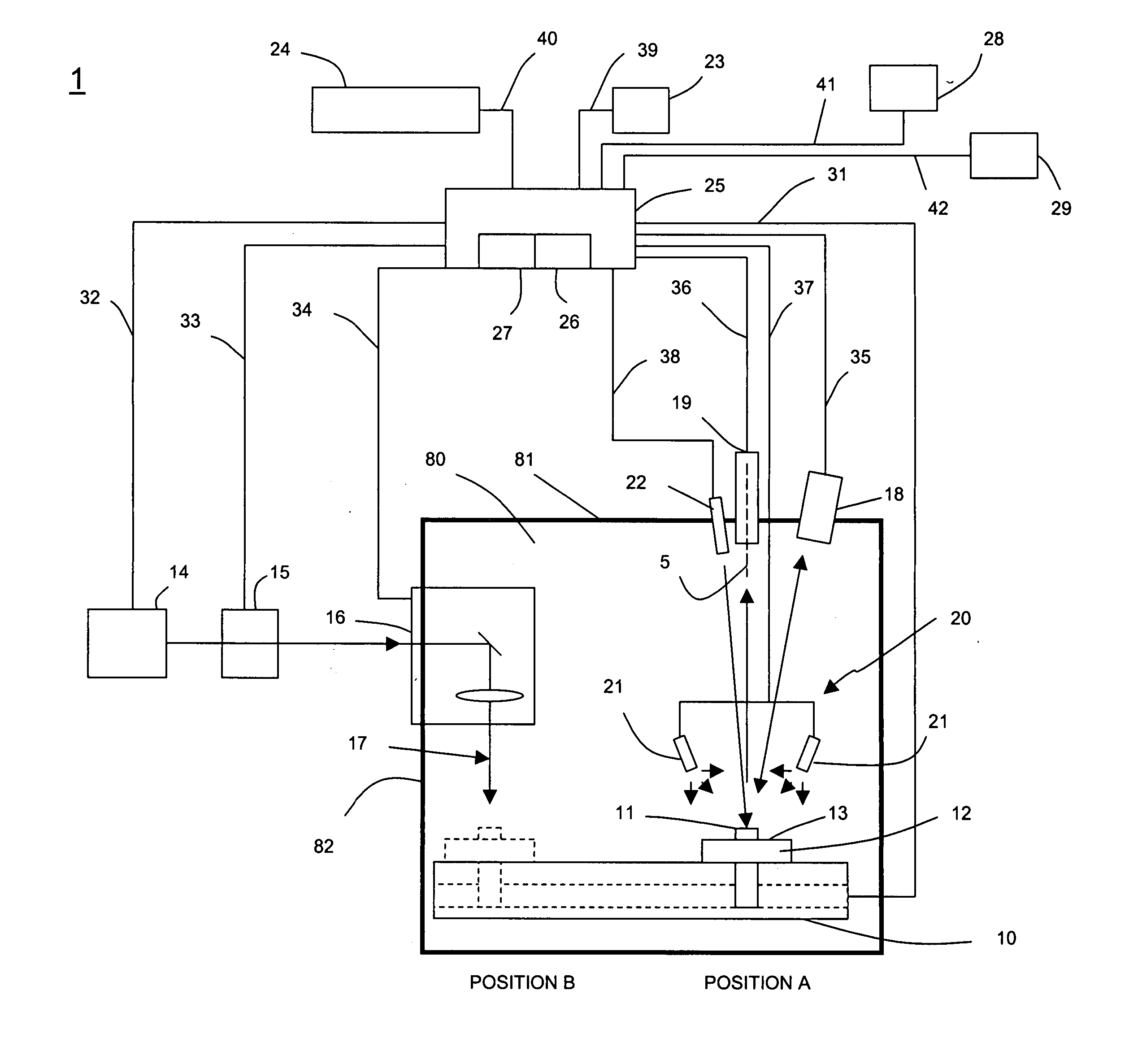
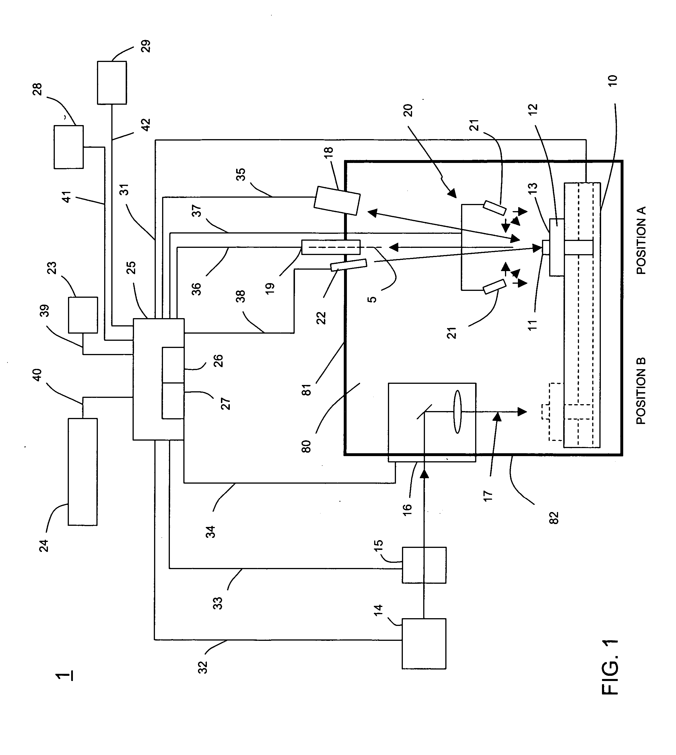
[0027] Failure analysis of packaged semiconductor devices requires that there be minimal damage to the device in order to perform tests and determine the causes of failures. In the past, damage-free decapsulation and cross-sectioning of packaged semiconductor devices by laser ablation has been difficult to achieve, in part because ablation threshold values differ among the various materials encountered in the removal process. Further, the most common package materials are not homogenous in nature. It has also been found that the density of package material can vary significantly as a function of depth from the upper surface of the package. Both the removal rate and the mechanisms of removal in an ablation process can vary depending on material properties and numerous variables associated with the ablation process. Relevant variables include laser wavelength, beam power, pulse width and scan speed. Ablation is also affected by presence of materials such as silica filler, commonly inc...


PUM

PropertyMeasurementUnit
angleaaaaaaaaaa
depth-to-widthaaaaaaaaaa
angleaaaaaaaaaa

Abstract

Systems and methods for removing material from a packaged electronic device of the type encapsulated with a protective material that forms an outer surface of the device. An exemplary system includes a stage for placing the device in a first position for receiving laser radiation to remove the material by ablation, and for placing the device in a second position for viewing one or more features along the outer surface of the device. An optical system is configured to provide an exterior image, including one or more features along an exposed surface of the device, while the device remains in the second position. A viewing system displays a captured image of the device, including one or more features interior to the protective surface, overlayed with the exterior image for simultaneous viewing of both images so that a position of a first feature present in the captured image can be viewed in relation to a position of a second feature in the exterior image. The combination of the first feature position and the second feature position can be used to define a region of the device for material removal with a laser. In an associated method a captured image of the device is provided, the image including one or more features interior to the protective surface. One or more features along the outer surface of the device are viewed with an optical system while the device remains on a stage, the optical system providing an exterior image. The captured image is combined with the exterior image for simultaneous viewing so that the position of a first feature present in the captured image can be viewed in relation to the position of a second feature in the exterior image. A region is defined for decapsulation based on the position of the first feature relative to the position of the second feature.

Description

RELATED APPLICATIONS [0001] This application claims priority to U.S. 60 / 695,477 filed Jun. 30, 2005, which is incorporated herein by reference in its entirety.REFERENCE TO APPENDIX [0002] This application includes a Computer Program Listing Appendix on one compact disc containing the following files, all of which information is hereby incorporated herein by reference in the entirety: SIZE OF FILEDATE FILEFILE NAMEIN KILOBYTESCREATEDAboutDlg.asm287kb6 / 29 / 2006CameraThread.asm272kb6 / 29 / 2006CamSettingsDlg.asm61kb6 / 29 / 2006CleaningPassDlg.asm292kb6 / 29 / 2006CrossSectionDlg.asm292kb6 / 29 / 2006CSAMWnd.asm116kb6 / 29 / 2006CSISerial.asm17kb6 / 29 / 2006DecapView.asm506kb6 / 29 / 2006DigCtrl.asm145kb6 / 29 / 2006DrawObject.asm96kb6 / 29 / 2006DrawWnd.asm236kb6 / 29 / 2006FATCAT.asm565kb6 / 29 / 2006GProgressCtrl.asm93kb6 / 29 / 2006KnobCtrl.asm220kb6 / 29 / 2006LaserCalibration.asm676kb6 / 29 / 2006LaserControl.asm349kb6 / 29 / 2006LaserControlSHP.asm210kb6 / 29 / 2006LaserSettingsDlg.asm130kb6 / 29 / 2006MainFrm.asm727kb6 / 29 / 2006MainFrmCMD.asm37...

Claims


Application Information

Patent Timeline
Patent Type & Authority Applications(United States)
IPC IPC(8): B23K26/00
CPCB23K26/03B23K26/032H01L2924/1815H01L2224/73265H01L2224/49171H01L2224/48247H01L2224/48091H01L2224/32245H01L22/26B23K26/0665H01L2924/00014H01L2924/00
Inventor HEYL, JON
Owner CONTROLLED SEMICON
Why Eureka
Try Eureka