Self-aligned schottky-barrier clamped trench DMOS transistor structure and its manufacturing methods

a dmos power transistor and self-aligning barrier technology, which is applied in the direction of diodes, semiconductor devices, electrical apparatus, etc., can solve the problems of difficult scaling down the source area of the planar dmos power transistor, serious device reliability issues, etc., and achieve the effect of eliminating edge leakage curren

Inactive Publication Date: 2007-04-05
SILICON BASED TECH
View PDF4 Cites 77 Cited by
  • Summary
  • Abstract
  • Description
  • Claims
  • Application Information

AI Technical Summary

Benefits of technology

[0012] The present invention discloses a self-aligned Schottky-barrier clamped trench DMOS transistor structure and its manufacturing methods, in which a Schottky-barrier diode is integrated with each of trench DMOS transistor cells in a self-aligned manner. The self-aligned Schottky-barrier clamped trench DMOS transistor structure of the present invention comprises a self-aligned source region and a trench gate region, wherein the self-aligned source region is surrounded by the trench gate region. The self-aligned source region comprises a moderately-doped p-base diffusion ring being formed in a lightly-doped N− epitaxial semiconductor layer surrounded by the trench gate region, a heavily-doped n+ source diffusion ring being formed within the moderately-doped p-base diffusion ring, a self-aligned source contact window being formed on the lightly-doped N− epitaxial semiconductor layer surrounded by the moderately-doped p-base diffusion ring, the moderately-doped p-base diffusion ring being surrounded by the heavily-doped n+ source diffusion ring, and the heavily-doped n+ source diffusion ring being surrounded by a sidewall dielectric spacer formed over a sidewall of the trench gate region and on a side surface portion of a buffer dielectric layer in the self-aligned source region, and a self-aligned metal silicide layer being formed

Problems solved by technology

However, misalignments of the two critical masking photoresist steps may produce non-uniform current flow distribution, resultin

Method used


Image

  • Self-aligned schottky-barrier clamped trench DMOS transistor structure and its manufacturing methods
  • Self-aligned schottky-barrier clamped trench DMOS transistor structure and its manufacturing methods
  • Self-aligned schottky-barrier clamped trench DMOS transistor structure and its manufacturing methods

Examples


Embodiment Construction

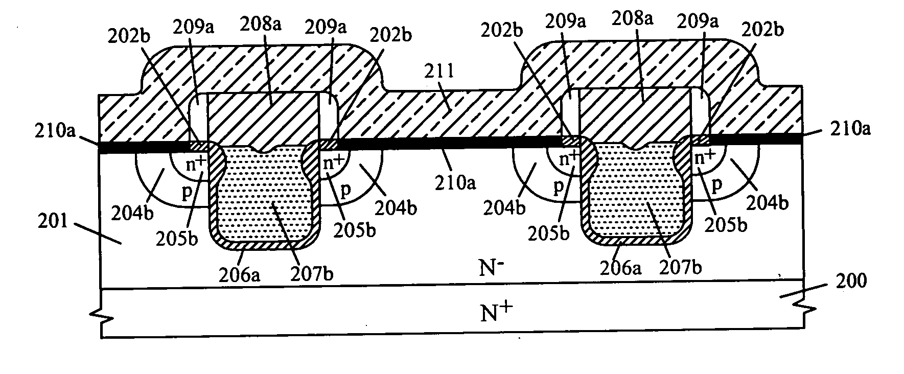
[0020] Referring now to FIG. 3A through FIG. 3G, there are shown process steps and their schematic cross-sectional views of fabricating a first-type self-aligned Schottky-barrier clamped trench DMOS transistor structure of the present invention.

[0021]FIG. 3A shows that a lightly-doped N− epitaxial silicon layer 201 is formed on a heavily-doped N+ silicon substrate 200; a buffer oxide layer 202 is then formed on the lightly-doped N− epitaxial silicon layer 201; subsequently, a masking dielectric layer 203 is formed on the buffer oxide layer 202; and thereafter, a first masking photoresist (PR1) step is performed to define a plurality of self-aligned source regions (SR) and a trench gate region (TGR) as shown in FIG.3B, wherein each of the plurality of self-aligned source regions (SR) is surrounded by the trench gate region (TGR).The heavily-doped N+ silicon substrate 200 is preferably to have a resistivity between 0.001 Ω*cm and 0.004 Ω*cm and a thickness between 300 μm and 800 μm, ...


PUM


Abstract

The self-aligned Schottky-barrier clamped trench DMOS transistor structure of the present invention comprises a Schottky-barrier diode being formed in a middle semiconductor portion of a self-aligned source region. The self-aligned source region comprises a lightly-doped epitaxial semiconductor layer, a moderately-doped base diffusion ring being formed in a surface portion of the lightly-doped epitaxial semiconductor layer surrounded by a trench gate region, a heavily-doped source diffusion ring being formed in a side surface portion of the moderately-doped base diffusion ring, and a self-aligned source contact being formed on a semiconductor surface of the self-aligned source region surrounded by a sidewall dielectric spacer. The trench gate region comprises a self-aligned conductive gate layer being formed over a gate dielectric layer lined over a trenched semiconductor surface in a shallow trench with or without a thicker isolation dielectric layer being formed on a bottom surface of the shallow trench.

Description

BACKGROUND OF THE INVENTION [0001] 1. Field of the Invention [0002] The present invention is generally related to a trench DMOS transistor structure and its manufacturing methods and, more particularly, to a self-aligned Schottky-barrier clamped trench DMOS transistor structure and its manufacturing methods. [0003] 2. Description of the Prior Art [0004] A DMOS (double-diffused metal-oxide-semiconductor) power transistor with a low turn-on resistance becomes an important semiconductor device for applications in battery protection, switching, linear regulator, amplifier and power management. [0005]FIG. 1A shows a schematic cross-sectional view for a non-self-aligned source structure of a prior-art planar DMOS transistor, in which a p-body diffusion region 104a is formed in a lightly-doped N− epitaxial silicon layer 101 formed on a heavily-doped N+ silicon substrate 100 through a patterned window surrounded by a patterned polycrystalline-silicon gate layer 103a on a gate oxide layer 10...

Claims


Application Information

Patent Timeline
IPC IPC(8): H01L29/76H01L29/94H01L31/00
CPCH01L29/42368H01L29/456H01L29/47H01L29/4925H01L29/4933H01L29/66719H01L29/66734H01L29/7806H01L29/7813
Inventor WU, CHING-YUAN
Owner SILICON BASED TECH
Why Eureka
Try Eureka