Self-aligned schottky-barrier clamped planar DMOS transistor structure and its manufacturing methods

Inactive Publication Date: 2006-06-22
SILICON BASED TECH
View PDF1 Cites 19 Cited by
  • Summary
  • Abstract
  • Description
  • Claims
  • Application Information

AI Technical Summary

Benefits of technology

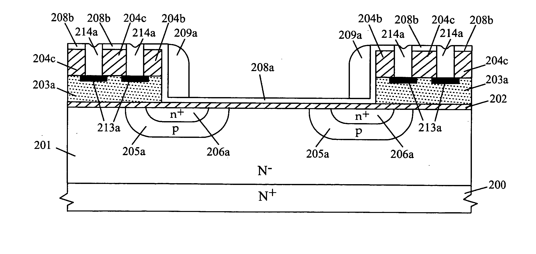
[0012] The present invention discloses a self-aligned Schottky-barrier clamped planar DMOS transistor structure and its manufacturing methods, in which a Schottky-barrier diode is integrated with each of planar DMOS transistor cells in a self-aligned manner. The self-aligned Schottky-barrier clamped planar DMOS transistor structure of the present invention comprises a self-aligned source region and a planar gate region, wherein the self-aligned source region is surrounded by the planar gate region. The self-aligned source region comprises a moderately-doped p-base diffusion ring being formed in a lightly-doped N− epitaxial semiconductor layer through a patterned window, a heavily-doped n+ source diffusion ring being formed within the moderately-doped p-base diffusion ring through the patterned window, a self-aligned Schottky-barrier contact window being formed on the lightly-doped N− epitaxial semiconductor layer surrounded by the moderately-doped p-base diffusion ring, the moderately-doped p-base diffusion ring being surrounded by the heavily-doped n+ source diffusion ring, and the heavily-doped n+ source diffusion ring being surrounded by a sidewall dielectric spacer formed over a sidewall of a protection dielectric layer and on a side surface portion of the protection dielectric layer in the self-aligned source region, and a self-aligned metal silicide layer being formed on the self-aligned Schottky-barrier contact window. The planar gate region comprises a pat

Problems solved by technology

However, misalignments of the two critical masking photoresist steps may produce non uniform current flow distribution, resultin

Method used


Image

  • Self-aligned schottky-barrier clamped planar DMOS transistor structure and its manufacturing methods
  • Self-aligned schottky-barrier clamped planar DMOS transistor structure and its manufacturing methods
  • Self-aligned schottky-barrier clamped planar DMOS transistor structure and its manufacturing methods

Examples


Embodiment Construction

[0019] Referring now to FIG. 3A through FIG. 3F, there are shown process steps and their schematic cross-sectional views of fabricating a first-type self-aligned Schottky-barrier clamped planar DMOS transistor structure of the present invention.

[0020]FIG. 3A shows a gate dielectric layer 202 is formed on an N− epitaxial silicon layer 201 being formed on an N+ silicon substrate 200; a heavily-doped polycrystalline-silicon layer 203 is then formed on the gate dielectric layer 202; a capping dielectric layer 204 is thereafter formed on the heavily-doped polycrystalline-silicon layer 203; and subsequently, a first masking photoresist (PR1) step is performed to define a plurality of implantation windows (IW). The N+ silicon substrate 200 is preferably to have a resistivity between 0.001 Ω*cm and 0.004 Ω*cm and a thickness between 300 μm and 800 μm, depending on wafer size. The N− epitaxial silicon layer 201 is preferably to have a resistivity between 100 Ω*cm and 0.1 Ω*cm and a thicknes...


PUM


Abstract

The self-aligned Schottky-barrier clamped planar DMOS transistor structure comprises a self-aligned source region being surrounded by a planar gate region. The self-aligned source region comprises a moderately-doped p-base diffusion ring being formed in a lightly-doped N epitaxial semiconductor layer, a heavily-doped n+ source diffusion ring being formed within the moderately-doped p-base diffusion ring, and a Schottky-barrier contact with the moderately-doped p-base diffusion ring acted as a diffusion guard ring being formed in a middle semiconductor surface portion of the self-aligned source region. The planar gate region comprises a patterned heavily-doped polycrystalline-silicon gate layer being silicided with or without metal silicide layers. The self-aligned source region further comprises a lightly-doped p diffusion region being formed beneath a middle portion of the moderately-doped p-base diffusion ring.

Description

BACKGROUND OF THE INVENTION [0001] 1. Field of the Invention [0002] The present invention relates generally to a planar DMOS power transistor and its manufacturing method and, more particularly, to a self-aligned Schottky-barrier clamped planar DMOS transistor structure and its manufacturing methods. [0003] 2. Description of the Prior Art [0004] A DMOS (double-diffused metal-oxide-semiconductor) power transistor with a low turn-on resistance becomes an important semiconductor device for applications in battery protection, switching, linear regulator, amplifier and power management. [0005]FIG. 1A shows a schematic cross-sectional view for a non-self-aligned source structure of a prior-art planar DMOS transistor, in which a p-body diffusion region 104a is formed in a lightly-doped n− epitaxial silicon layer 101 formed on a heavily-doped n+ silicon substrate 100 through a patterned window surrounded by a patterned polycrystalline-silicon gate layer 103a on a gate oxide layer 102a by us...

Claims


Application Information

Patent Timeline
IPC IPC(8): H01L29/80H01L29/76
CPCH01L27/0727H01L29/4933H01L29/66719H01L29/7806
Inventor WU, CHING-YUAN
Owner SILICON BASED TECH
Why Eureka
Try Eureka