Organic electroluminescent device and optical device

a technology of organic electroluminescent devices and optical devices, which is applied in the direction of discharge tubes/lamp details, discharge tubes luminescnet screens, incadescent body mounting/support, etc., can solve the problems of difficult to manufacture full color display panels, difficult to provide flat luminescent layers, and difficult to form low-molecular luminescent layers on large panels in uniform thickness. achieve the effect of increasing the numerical aperture of the organic electroluminescent device and increasing the numerical apertur

Inactive Publication Date: 2007-04-05
SEIKO EPSON CORP
View PDF12 Cites 37 Cited by
  • Summary
  • Abstract
  • Description
  • Claims
  • Application Information

AI Technical Summary

Benefits of technology

[0011] An advantage of the invention is that it provides an organic electroluminescent device having a flat luminescent layer formed by coating a coating solution containing an organic electroluminescent material on an anisotropic area such as a cylindrical form using an inkjet method and drying out the coating solution, and an optical device such as a color filter formed by coating a coating solution containing an optical material on an anisotropic area using an inkjet method in a similar way to the above organic electroluminescent device.
[0012] According to a first aspect of the invention, there is provided an organic electroluminescent device including: a panel; a partition that defines a plurality of hollows arranged in an anisotropic shape in a plan view on the panel; a luminescent portion formed by individually coating a coating solution containing an electroluminescent material on each of the plurality of hollows and drying out the coating solution coated on the hollows; and a drain means that is formed in the partition to drain part of the coating solution coated on the hollow so that a surface of the luminescent portion can be flattened.
[0013] In the organic electroluminescent device according to a first aspect of the invention, the partition defines, for example, a plurality of hollows that are individually formed on each pixel. More specifically, the partition electrically separates the luminescent layers formed by coating the coating solution containing the organic electroluminescent material on a plurality of hollows from each other. Each luminescent layer can independently emit light. For example, the luminescent layers are formed by coating the coating solution containing the organic electroluminescent materials capable of emitting red, green and blue colors on each of a plurality of the hollows so that a full color image can be displayed.
[0014] The luminescent layers are formed by coating the coating solution on each of the hollows using a coating method such as an inkjet method and drying out the coating solution coated on each hollow. Each of a plurality of hollows has an anisotropic shape in a plan view in order to increase a numerical aperture of the organic electroluminescent device. For example, the hollows having a cylindrical form defined by

Problems solved by technology

For this reason, it is thought that it is difficult to form the luminescent layer made of a low-molecular material on a large panel in a uniform thickness.
Therefore, it has been thought that it is difficult to manufacture a full color display panel by coating a coating solution containing luminescent materials for each color.
Therefore, it is technically difficult to provide a flat luminescent layer.
In consideration with the aforementioned technical problems, it is difficult to provide a luminescent layer having a sufficiently uniform thickness based on the JP-A-10-153967 and the JP-A-2002-252083.
Even when the technique disclosed in JP-A-2002-148429 is used, it is difficult to flatten the surface of the liquid droplet by adjusting the force applied from the side wall surface that defines the anisotropic area on which the liquid droplet is coated

Method used


Image

  • Organic electroluminescent device and optical device
  • Organic electroluminescent device and optical device
  • Organic electroluminescent device and optical device

Examples


first embodiment

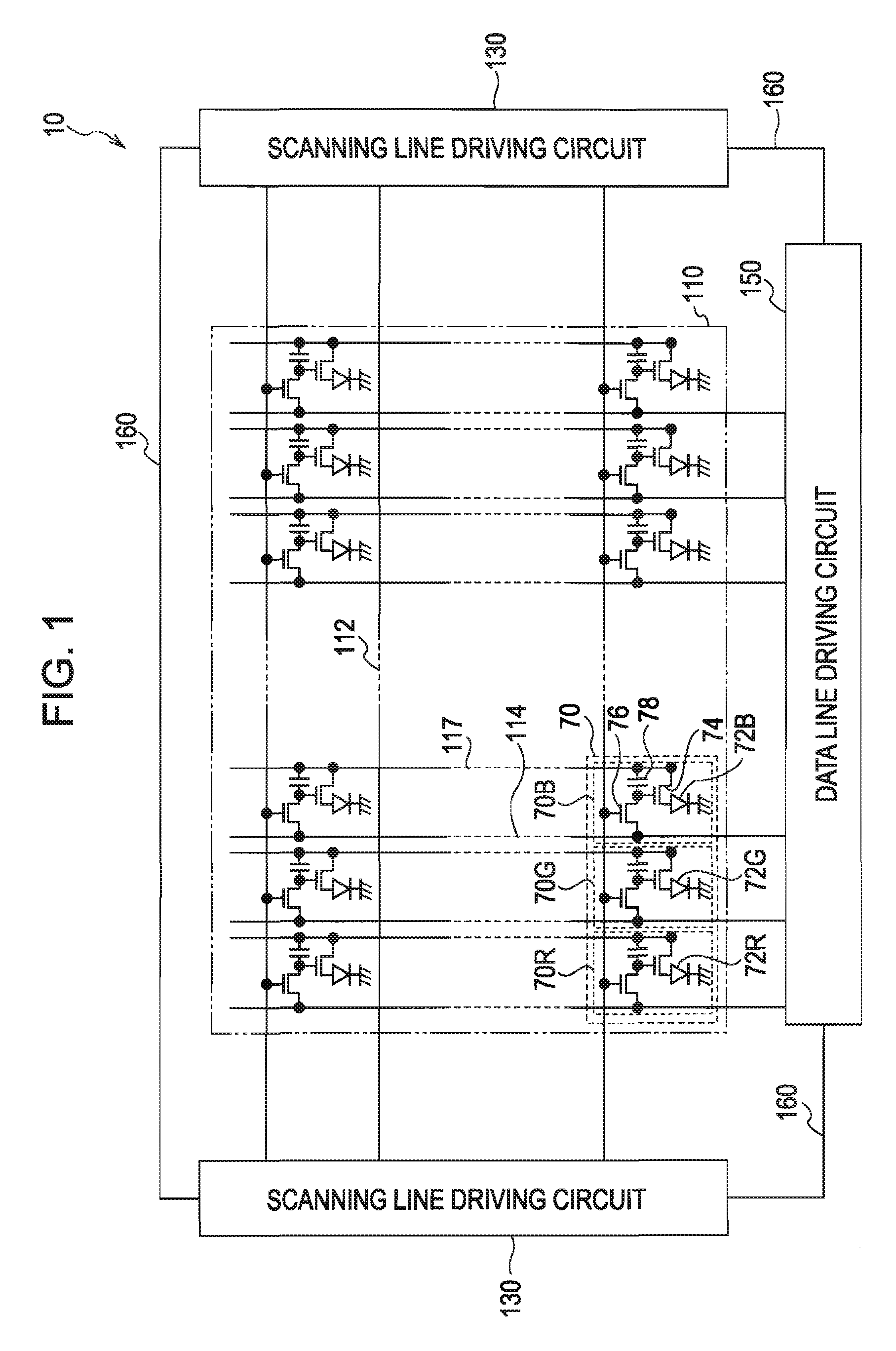
[0055] Firstly, an organic electroluminescent device according a first embodiment of the invention will be described with reference to FIGS. 1 to 7. FIG. 1 is a block diagram illustrating an entire construction of an organic electroluminescent device according to a first embodiment of the invention.

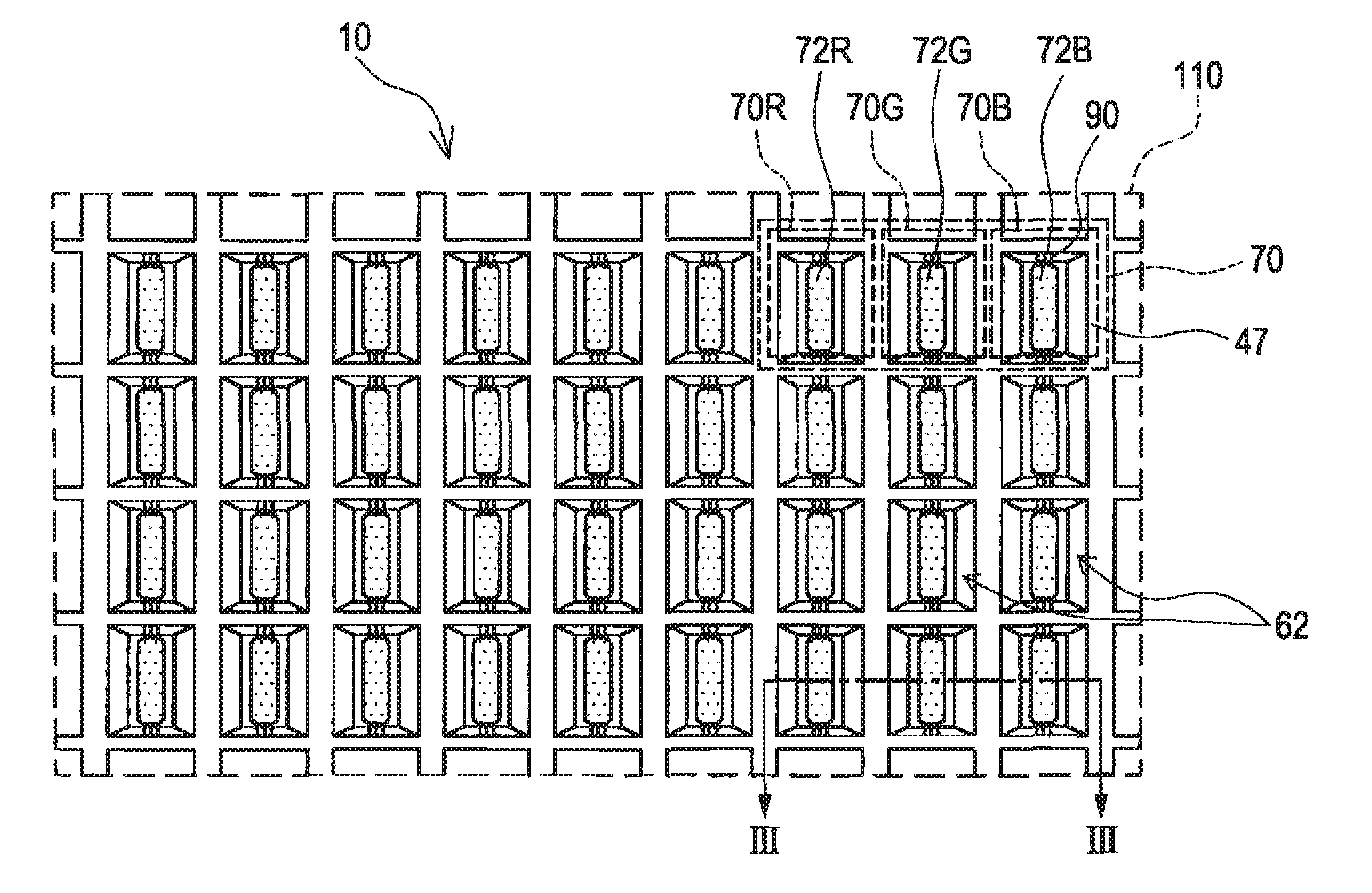
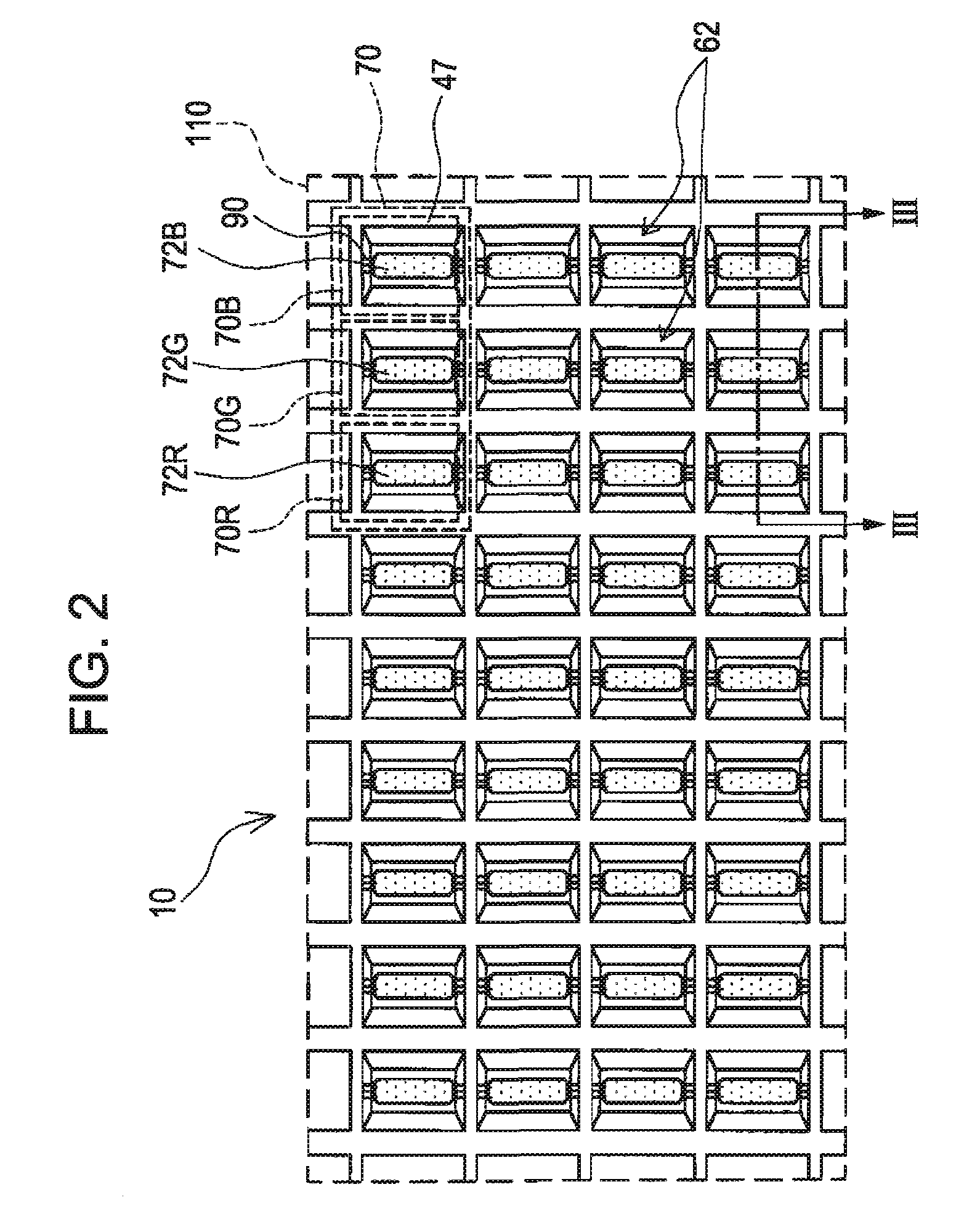
[0056] Referring to FIG. 1, the organic electroluminescent device 10 is an active matrix type display device having an embedded driving circuit, and each pixel 70 included in the organic electroluminescent device 10 includes an organic electroluminescent element 72.

[0057] Data lines and scanning lines extending across each other in vertical and horizontal directions are arranged in the pixel area 110 of the organic electroluminescent device 10. The subpixels 70R, 70G and 70B provided in each intersection are arranged in a matrix form, and a set of three subpixels constitutes one pixel 70. The subpixels 70R, 70G and 70B have organic electroluminescent elements 72R, 72G, and 72B emitting ...

second embodiment

[0084] An organic electroluminescent device according to a second embodiment of the invention will now be described with reference to FIGS. 10 and 11. FIG. 10 is a plan view illustrating an organic electroluminescent device 300 according to a second embodiment of the invention.

[0085] Referring to FIG. 10, an organic electroluminescent device 300 includes a plurality of pixels 70 having an organic electroluminescent layer 50 formed using an inkjet method. The dry rate of the coating solution coated on the hollow 62 defined by the bank 47 is different between a group of pixels 70b arranged near the edges of the panels 301 and a group of pixels 70a arranged near the center of the panel 301 among a plurality of pixels 70 included in a pixel area. More specifically, even when a drying condition is accurately controlled as the size of the panel 301 becomes large, the dry rate of the coating solution of a group of the pixels 70b is relatively faster than that of a group of the pixels 70a....


PUM


Abstract

Disclosed is an organic electroluminescent device including: a panel; a partition that defines a plurality of hollows arranged in an anisotropic form in a plan view on the panel; a luminescent portion formed by individually coating a coating solution containing an electroluminescent material on each of the plurality of hollows and drying out the coating liquid coated on the hollows; and a drain means that is formed in the partition to drain part of the coating liquid coated on the hollow so that a surface of the luminescent portion can be flattened.

Description

BACKGROUND [0001] 1. Technical Field [0002] The present invention relates to an organic electroluminescence device such as an organic electroluminescence display unit manufactured using, for example, an inkjet method and an optical device such as a color filter. [0003] 2. Related Art [0004] In an organic electroluminescent device manufactured using an inkjet method, a low-molecular luminescent material or a polymer luminescent material is used to form an organic electroluminescent layer as a light-emitting layer. The luminescent layer formed of the low-molecular luminescent material is typically formed using a dry method such as a vacuum deposition method. For this reason, it is thought that it is difficult to form the luminescent layer made of a low-molecular material on a large panel in a uniform thickness. The luminescent layer made of a polymer material is typically formed by coating a coating solution obtained by diffusing and dissolving the polymer luminescent material in a so...

Claims


Application Information

Patent Timeline
IPC IPC(8): H01L51/00
CPCH01L27/3246H01L51/0004H01L51/56H10K59/122H10K71/13H10K71/00H05B33/22H05B33/10
Inventor MITSUYA, MASAYUKI
Owner SEIKO EPSON CORP
Why Eureka
Try Eureka