This helps you quickly interpret patents by identifying the three key elements:
Problems solved by technology
Method used
Benefits of technology
Benefits of technology
[0015] It is therefore an object of the present invention to overcome the problem with the conventional example and to provide a buck-boost converter in which on and off operations are not performed within one switching cycle to thereby separate buck converter operation and boost converter operation, while transitions between the buck converter operation and the boost converter operation are made smoothly to thereby prevent increase in output ripple during the transition periods.
[0030] As described above, in the inventive buck-boost converter, the control signal obtained by adding together the error signal and the compensatory signal is compared with the triangular wave signal produced by the oscillator circuit. Therefore, in the transition periods between the boost converter operation and the buck converter operation, switching between the boost converter operation and the buck converter operation is made in accordance with the cycles of the compensatory signal. This avoids irregular switching between the through mode and the boost or buck operation, while preventing the first and second switches from performing the on and off operations within one switching cycle. As a result, it is possible to separate the operation of the buck converter section and the operation of the boost converter section, thereby enabling smooth transitions between the boost operation and the buck operation.
Problems solved by technology
In the real world, the operation of the buck-boost converter is not stable in the through mode, and slight variation in input / output conditions and environment causes switching between the through mode and the boost or buck operation.
Such transient changes in the operation state are also affected by response speed of the control circuit 30 including the error amplifier circuit 31 and the like and are thus irregular, thereby causing a problem in that the output ripple of the output DC voltage Vo is increased.
Method used
Image
Click on the blue label to locate the original text in one second.
Reading with bidirectional positioning of images and text.
Examples
first embodiment
[0047] A buck-boost converter according to a first embodiment of the present invention will be described with reference to the accompanying drawings.
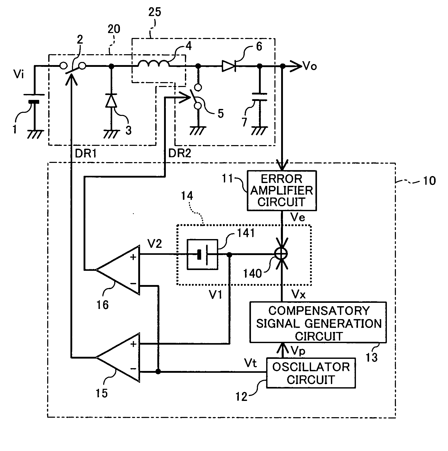
[0048]FIG. 1 shows the circuit configuration of the buck-boost converter according to the first embodiment of the present invention. As shown in FIG. 1, the buck-boost converter of the first embodiment includes: a buck converter section 20, which includes a first switch 2, a first diode 3 serving as first rectifier means, and an inductor 4; a boost converter section 25, which shares the inductor 4 and includes a second switch 5, a second diode 6 serving as second rectifier means, and a capacitor 7 serving as smoothing means; and a control circuit 10, which generates and outputs a first driving signal DR1 for opening and closing the first switch 2 and a second driving signal DR2 for opening and closing the second switch 5. As the first switch 2 and the second switch 5, MOS transistors may be used, for example.
[0049] In the buck convert...
second embodiment
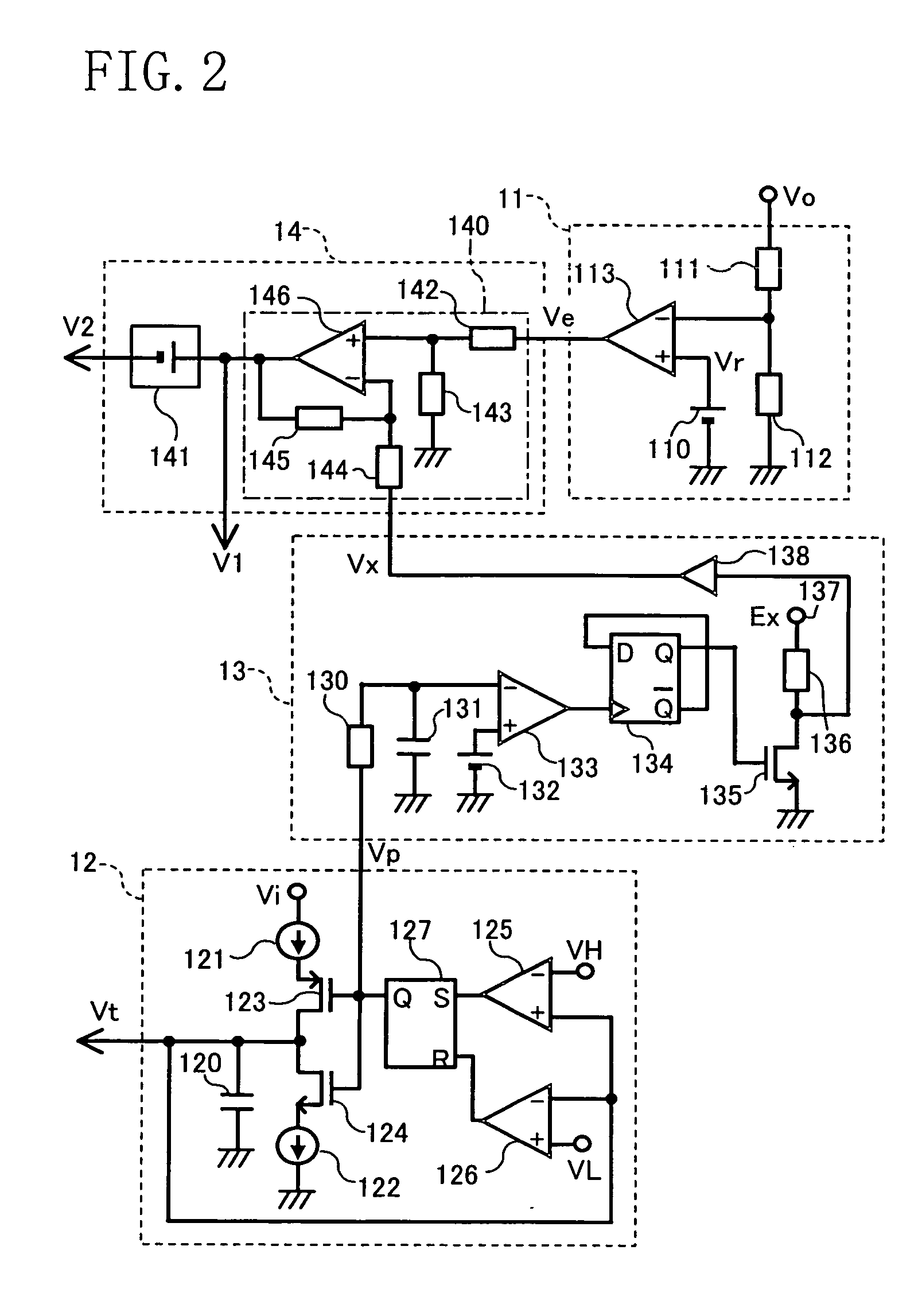
[0071] Hereinafter, a buck-boost converter according to a second embodiment of the present invention will be described with reference to the accompanying drawings.
[0072]FIG. 4 shows the circuit configuration of the buck-boost converter according to the second embodiment of the present invention. In FIG. 4, the same members as those of the buck-boost converter shown in FIG. 1 are identified by the same reference numerals and the description thereof will be thus omitted herein.
[0073] The buck-boost converter according to the second embodiment includes a control circuit 10A which is different in configuration from the control circuit 10 of the first embodiment.
[0074] As shown in FIG. 4, the control circuit 10A of the second embodiment includes: an error amplifier circuit 11A composed of an error amplifier 114 and an offset voltage source 115; a compensatory signal generation circuit 13A; and a control signal generation circuit 14A.
[0075] The error amplifier 114 of the error amplifi...
third embodiment
[0089] Hereinafter, a buck-boost converter according to a third embodiment of the present invention will be described with reference to the accompanying drawings.
[0090]FIG. 7A shows the circuit configuration of the buck-boost converter according to the third embodiment of the present invention. In FIG. 7A, the same members as those of the buck-boost converter shown in FIG. 1 are identified by the same reference numerals and the description thereof will be thus omitted herein.
[0091] The buck-boost converter according to the third embodiment includes a control circuit 10B which is different in configuration from the control circuit 10 of the first embodiment.
[0092] As shown in FIG. 7A, the control circuit 10B of the third embodiment includes: an oscillator circuit 12B, a compensatory signal generation circuit 13B; a control signal generation circuit 14B; a first comparator 15B; and a second comparator 16B.
[0093] The oscillator circuit 12B includes a signal generation circuit 220 a...
PUM
Abstract
A buck-boost converter includes: a buck converter section including a first switch, a first rectifier, and an inductor; a boost converter section sharing the inductor and including a second switch, a second rectifier, and a smoothing circuit; and a control circuit for generating and outputting a first driving signal for opening and closing the first switch and a second driving signal for opening and closing the second switch. The control circuit includes:an error amplifier circuit for amplifying an error between an output value from the smoothing circuit and a predetermined voltage value to thereby generate and output an error signal; an oscillator circuit for generating and outputting a triangular wavesignal having a predetermined cycle; a compensatory signal generation circuit for generating and outputting a compensatory signal, which oscillates in a cycle that is at least twice the cycle of the triangular wave signal; a control signal generation circuit for adding together the error signal and the compensatory signal to thereby generate and output a control signal; and a comparator circuit for comparing the triangular wave signal with the control signal to generate and output the first or second driving signal.
Description
CROSS-REFERENCE TO RELATED APPLICATION [0001] The disclosure of Japanese Patent Application No. 2005-286218 filed on Sep. 30, 2005 including specification, drawings and claims is incorporated herein by reference in its entirety. BACKGROUND OF THE INVENTION [0002] The present invention relates to a non-isolated buck-boost converter for converting an input DC voltage to a predetermined output voltage. [0003] In a power supply circuit which receives a DC voltage (hereinafter referred to as an “input DC voltage”) from a DC power supply and outputs a DC voltage (hereinafter referred to as an “output DC voltage”) as a DC power supply voltage for various kinds of electronic circuits, a buck-boost converter is used when the input DC voltage varies with respect to the predetermined output DC voltage. Such a buck-boost converter is described in Japanese Laid-Open Publication No. 11-299229, for example. [0004] Hereinafter, with reference to FIG. 12, the buck-boost converter described in the ab...
Claims
Application Information
Patent Timeline
Application Date:The date an application was filed.
Publication Date:The date a patent or application was officially published.
First Publication Date:The earliest publication date of a patent with the same application number.
Issue Date:Publication date of the patent grant document.
PCT Entry Date:The Entry date of PCT National Phase.
Estimated Expiry Date:The statutory expiry date of a patent right according to the Patent Law, and it is the longest term of protection that the patent right can achieve without the termination of the patent right due to other reasons(Term extension factor has been taken into account ).
Invalid Date:Actual expiry date is based on effective date or publication date of legal transaction data of invalid patent.

