Multilevel interconnection board and method of fabricating the same

Inactive Publication Date: 2007-04-05
FUJITSU LTD
View PDF3 Cites 13 Cited by
  • Summary
  • Abstract
  • Description
  • Claims
  • Application Information

AI Technical Summary

Benefits of technology

[0009] It is therefore an object of the present invention to provide a multilevel interconnection board

Problems solved by technology

The multilevel interconnection board may, however, be suffered from warping or cracking even if the above-described structure is adopted, due to internal stress concentrated at the interface at a temperature as high as around 150° C. The board may a

Method used


Image

  • Multilevel interconnection board and method of fabricating the same
  • Multilevel interconnection board and method of fabricating the same
  • Multilevel interconnection board and method of fabricating the same

Examples


Example

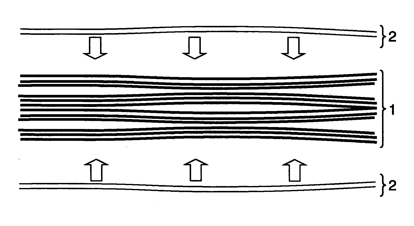
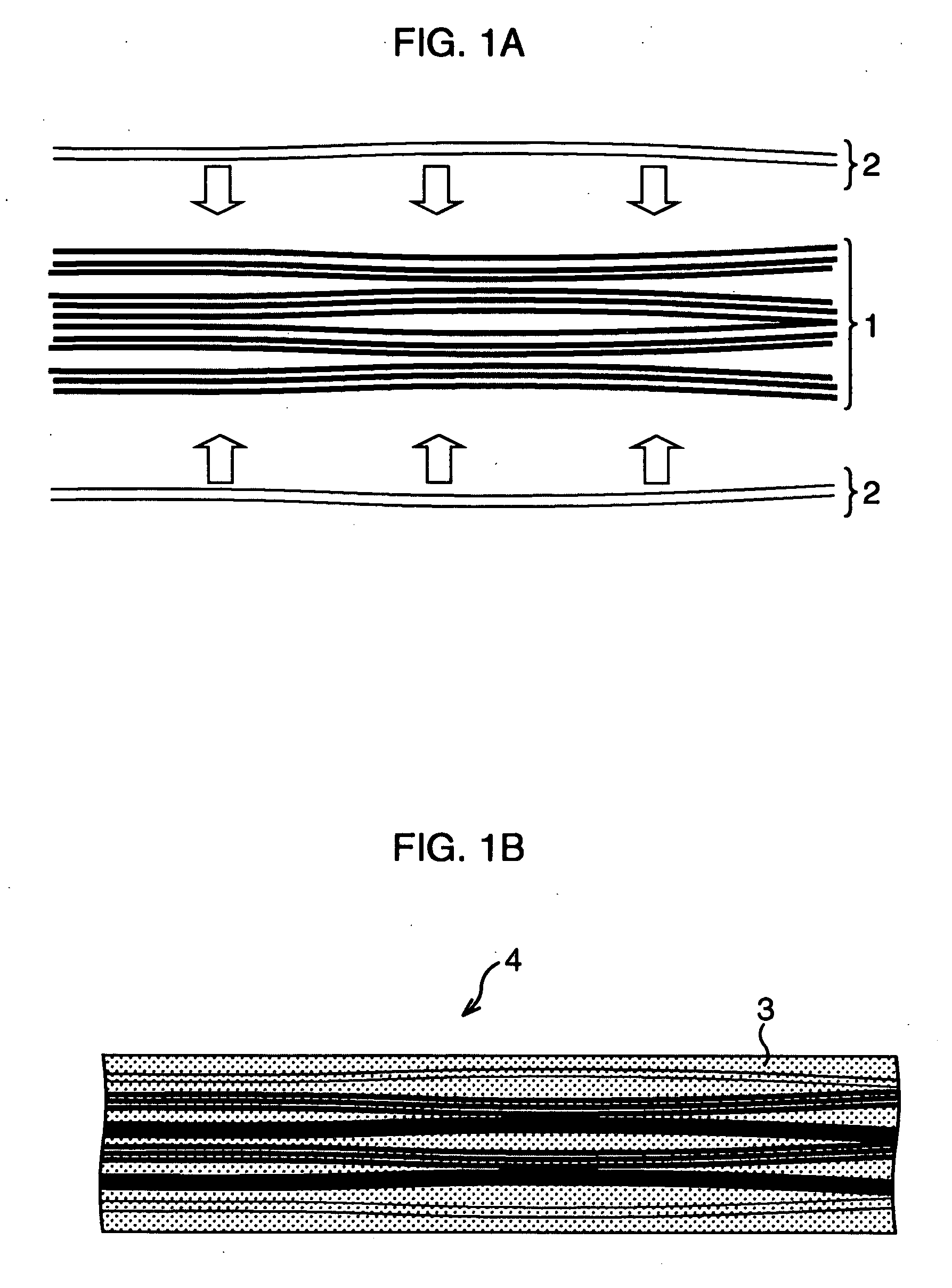
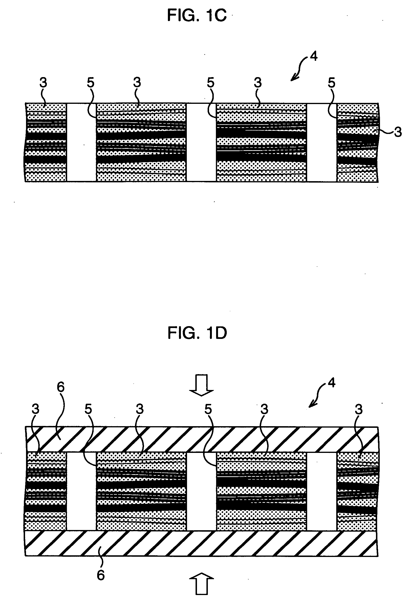
[0013] Paragraphs below will specifically explain embodiments of the present invention, referring to the attached drawings. It is to be noted that a structure of the multilevel interconnection board will be described in conjunction with a method of fabrication of the same for the convenience's sake. FIGS. 1A to 1L are sectional views sequentially showing process steps of the method of fabrication of the multilevel interconnection board according to the embodiment of the present invention.

[0014] In this embodiment, a stack (first carbon fiber group) having stacked therein 50 pitch-base, plain-woven carbon fiber sheets 1, each having an areal weight of carbon fiber of 300 g / m2 and a tensile elastic constant of 600 GPa, is formed. Two sets of stack (second carbon fiber group), each having stacked therein two pitch-base unidirectionally-woven carbon fiber sheets 2, for example, having an areal weight of carbon fiber of 100 g / m2 and a tensile elastic constant of 400 GPa, are formed. The...


PUM

PropertyMeasurementUnit
Densityaaaaaaaaaa
Purityaaaaaaaaaa
Thermal expansion coefficientaaaaaaaaaa

Abstract

A stack of 50 layers of a first pitch-base carbon fiber sheet is formed, two sets of stack each having two second pitch-base carbon fiber sheets stacked therein are fabricated. At this time, the second carbon fiber sheets have a thermal expansion coefficient larger than that of the first carbon fiber sheet. Next, the stack of the first carbon fiber sheet is then held between two sets of stack of the second carbon fiber sheets. The stack of the first and second carbon fiber sheets are then impregnated with an epoxy-base resin composition and the resin is solidified. As a result a prepreg composed of the first and second carbon fiber sheets and the resin component composed of the epoxy-base resin composition is obtained. Thereafter, interconnections and the like are then formed on the prepreg, to thereby complete a multilevel interconnection board.

Description

CROSS-REFERENCE TO RELATED APPLICATIONS [0001] This application is based upon and claims the benefit of priority from the prior Japanese Patent Application No. 2005-290357, filed on Oct. 3, 2005, the entire contents of which are incorporated herein by reference. BACKGROUND OF THE INVENTION [0002] 1. Field of the Invention [0003] The present invention relates to a multilevel interconnection board used for testing semiconductor devices and so forth, and a method of fabricating the same. [0004] 2. Description of the Related Art [0005] Tester board (multilevel interconnection board) is used typically in electrical tests of wafers having semiconductor devices formed thereon, in order to make contact between probes and terminals of each semiconductor device. A high level of dimensional accuracy is required for the multilevel interconnection board, because the probes and terminals are disposed at extremely narrow intervals. With recent increase in size of wafers, an extremely high dimensio...

Claims


Application Information

Patent Timeline
IPC IPC(8): B32B5/26B32B3/12B32B7/02B32B7/027
CPCB32B3/02Y10T428/24942B32B5/26B32B7/02B32B27/08B32B27/12B32B27/281B32B2250/05B32B2255/10B32B2255/205B32B2260/021B32B2260/046B32B2262/101B32B2262/106B32B2307/308B32B2307/734B32B2457/00H05K1/036H05K1/0366H05K3/429H05K3/4641H05K2201/0323H05K2201/068H01L2924/0002B32B5/024Y10T428/24149H01L2924/00Y10T428/24994Y10T442/696Y10T428/249945Y10T428/249923Y10T442/697Y10T442/643Y10T442/668Y10T442/659B32B7/027
Inventor OKAMOTO, KEISHIROKURASHINA, MAMORUABE, TOMOYUKI
Owner FUJITSU LTD
Why Eureka
Try Eureka