Method of producing circuit carriers with integrated passive components

a passive component and circuit carrier technology, applied in the direction of printed resistor incorporation, conductive pattern formation, printed element electric connection formation, etc., can solve the problem of high cost, high capacitance value, and said stability is normally not sufficient to realize larger areas, etc., to achieve rapid and inexpensive manufacture and high flexibility in selection

Inactive Publication Date: 2007-04-05
FRIWO GERAETEBAU GMBH
View PDF10 Cites 1 Cited by
  • Summary
  • Abstract
  • Description
  • Claims
  • Application Information

AI Technical Summary

Benefits of technology

[0012] It is therefore the object of the present invention to provide an improved method for producing an electrical subassembly with a circuit carrier and at least one passive component integrated i

Problems solved by technology

This process, however, is very troublesome and entails high costs.
Nevertheless, said stability is normally not sufficient for realizing larger areas and thus higher capacitance values.
The production of such capacitors, however, is c

Method used


Image

  • Method of producing circuit carriers with integrated passive components
  • Method of producing circuit carriers with integrated passive components
  • Method of producing circuit carriers with integrated passive components

Examples


first embodiment

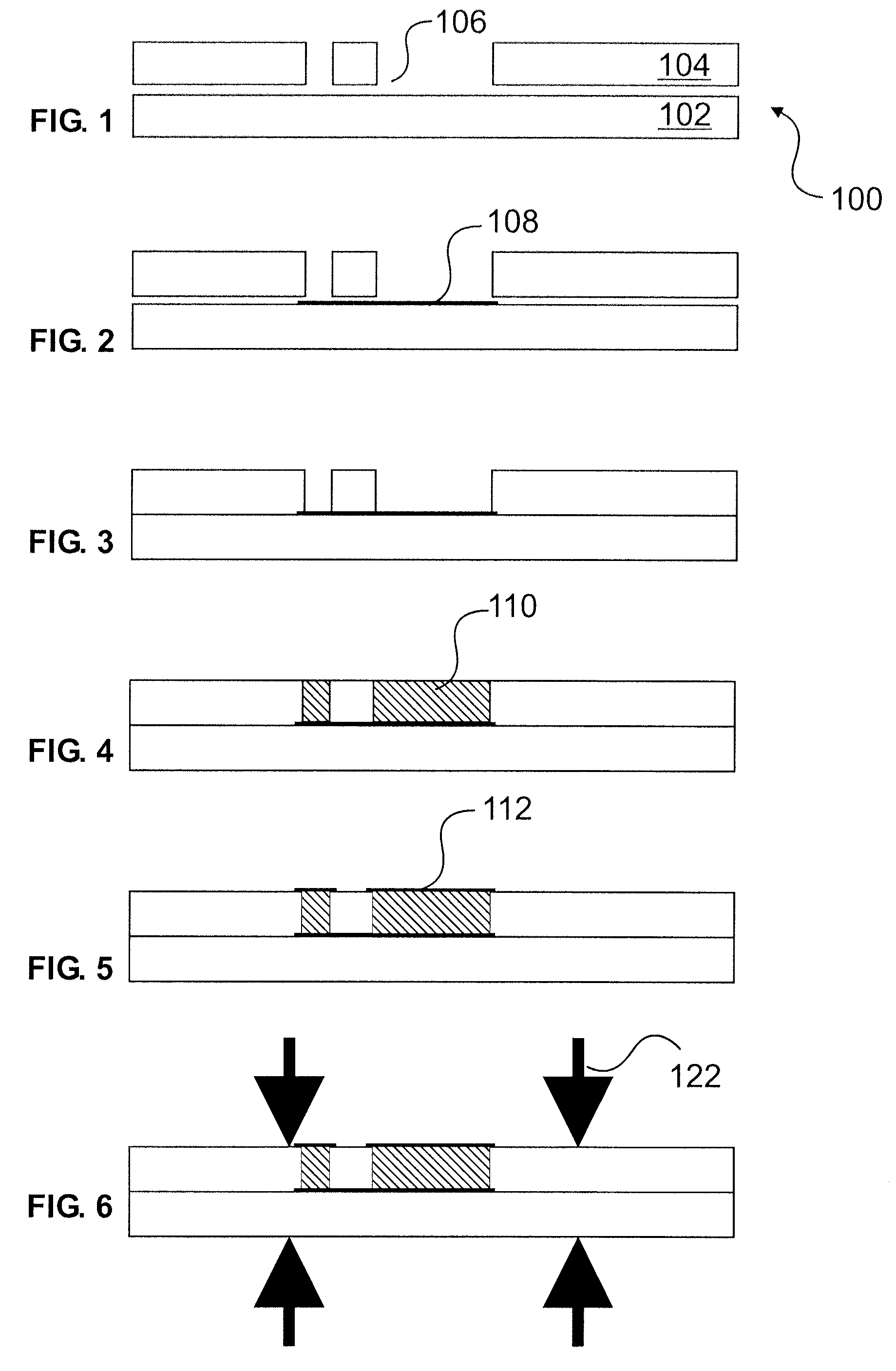
[0060] With reference to FIGS. 1 to 6 the manufacturing method according to the invention shall now be explained in more detail with reference to a

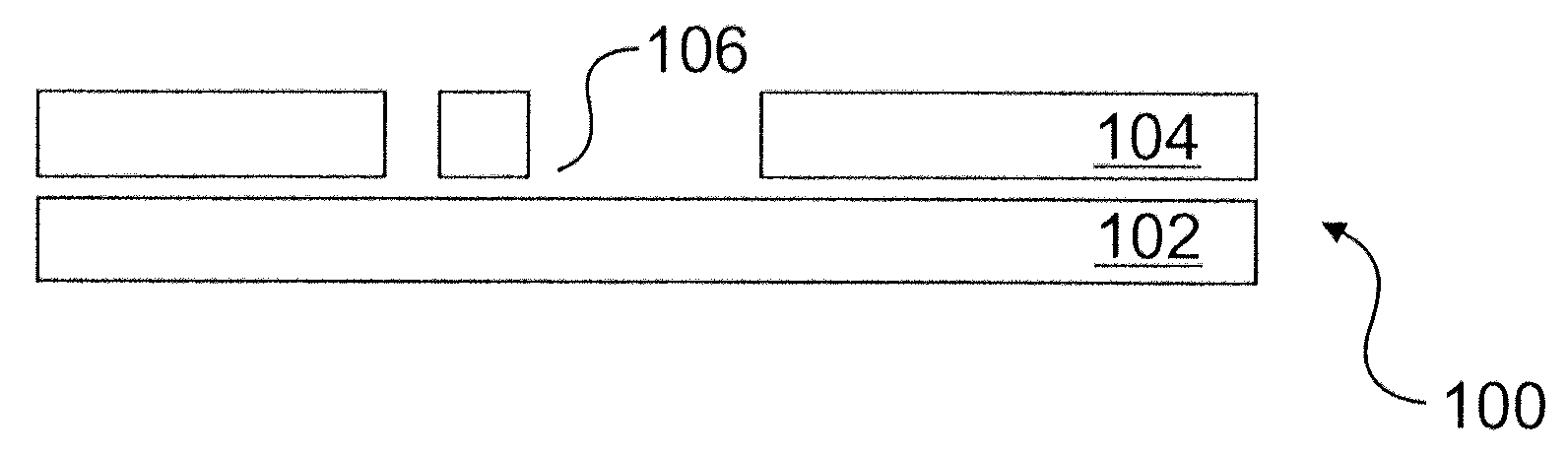
[0061] In the method according to the first embodiment a subassembly is produced with different integrated capacitors and a circuit carrier of ceramics. The ceramic substrates can provide great heat dissipation. They are structured and metallized such that free spaces are created for a dielectric substance in the raw state. This substance is introduced into the free spaces and the stacked ceramic substrates are pressed and sintered. The dielectric can be contacted from both sides. FIG. 1 shows a first ceramic layer 102 and a second ceramic layer 104 before these are joined to form a circuit carrier 100. The first ceramic layer 102 serves as a base layer and the second ceramic layer 104 is structured such that recesses 106 are created for later introduction of the dielectric.

[0062] As can be seen from FIG. 2, for contacting the later capa...

second embodiment

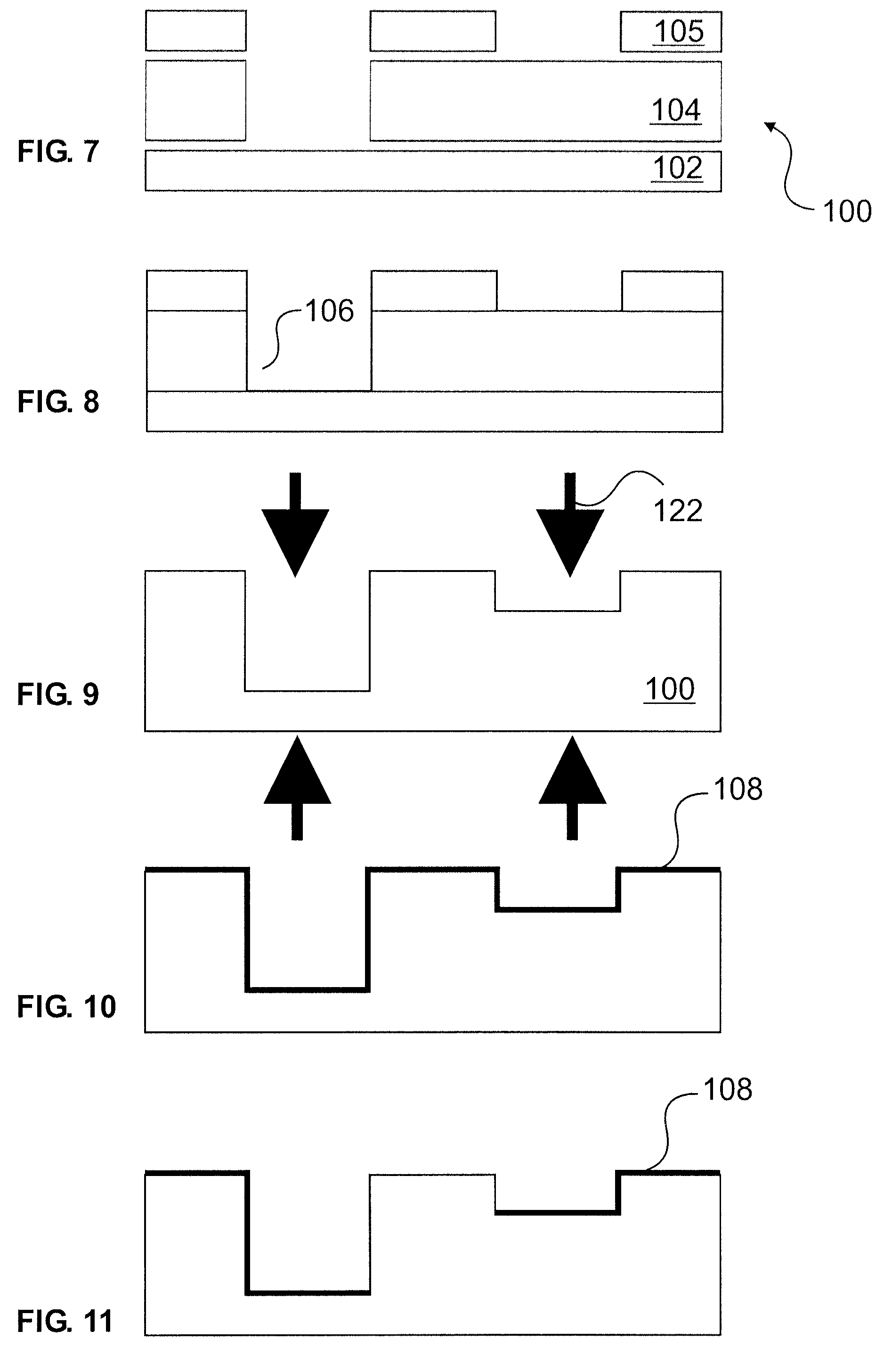
[0067] FIGS. 7 to 15 explain a method with the help of which passive components of a different thickness can also be produced.

[0068] First of all, as shown in FIGS. 7 to 9, a ceramic substrate 100 is produced by the measure that individual ceramic layers 102, 104, and 105 are structured, stacked and pressed and fired.

[0069] Said ceramic substrate 100 is fully metallized on the structured side, the metallization 108 is structured by photo-structured etching or in a process similar to the damascene method (FIGS. 10 and 11).

[0070] The dielectric 112 is then introduced in the raw state into the free spaces 106 provided for (FIG. 12). A second firing operation is carried out, shown by symbols in FIG. 13. Subsequently, the still missing contact surfaces are produced by a second metallization layer 112 to be structured (FIGS. 14 and 15).

[0071] The first firing operation for the substrate can take place at an elevated temperature because no metals are here needed. Therefore, said first ...

fourth embodiment

[0080] the method according to the invention is shown in FIGS. 24 to 31.

[0081] A pressing and firing operation of the ceramic substrate 100 is first of all performed (FIG. 24). As shown in FIG. 25, the ceramic is structured “from the solid block”, e.g. by milling or a laser treatment. By analogy with the process steps of FIGS. 10 to 15, the steps metallization, structuring of the metallization, introduction of the dielectric and a further pressing and firing operation are then performed (FIGS. 26 through 29). The missing contacts have now to be metallized again. This can be done either with the help of a mask by a photo technique, first with a complete metallization and a subsequent etching operation or by means of a damascene technique.

[0082] In all of the illustrated embodiments of the manufacturing process according to the invention, silver palladium or another conductive material with a melting temperature of more than 1300° C. can be used for the first metallization 108 and / or...


PUM

PropertyMeasurementUnit
Timeaaaaaaaaaa
Pressureaaaaaaaaaa
Electrical resistanceaaaaaaaaaa

Abstract

The present invention relates to a method for producing an electrical subassembly comprising a circuit carrier and at least one passive component which is integrated into the circuit carrier and comprises an electrically functional material. For providing an improved method for manufacturing an electrical subassembly comprising a circuit carrier and at least one passive component integrated into the circuit carrier, the method ensuring a rapid and inexpensive manufacture on the one hand and permitting a high flexibility on the other hand in the selection of the electrically functional materials involved, the method comprising structuring the circuit carrier, at least one recess being created for the passive element; introducing the electrically functional material in a raw state into the recess of the circuit carrier; converting the electrically functional material from the raw state into a final state by supplying energy.

Description

RELATED APPLICATIONS [0001] This patent application is a divisional of U.S. patent application Ser. No. 10 / 730,374 filed Dec. 8, 2003.BACKGROUND [0002] 1. Field of the Invention [0003] The present invention relates generally to the production of electronic circuits. More particularly, the present invention relates to a method for producing an electrical subassembly comprising a circuit carrier and at least one passive component which is integrated into the circuit carrier and comprises an electrically functional material. [0004] 2. Description of the Related Art [0005] In many electronic devices, passive components, such as resistors and capacitors or also inductors, are nowadays needed within a space that is as narrow as possible. Capacitors are e.g. used for suppressing noise, for filtering signals or for storing energy. Different techniques can be used for production. While for reasons of costs wound electrolyte capacitors are still used nowadays for capacitors having high capaci...

Claims


Application Information

Patent Timeline
IPC IPC(8): H01L21/00H01L21/02H01L27/08H05K1/03H05K1/09H05K1/16H05K3/06H05K3/10H05K3/12H05K3/40H05K3/46
CPCH01L27/08Y10T29/49128H05K1/0306H05K1/092H05K1/162H05K1/167H05K3/06H05K3/107H05K3/1258H05K3/4061H05K3/4611H05K3/4629H05K2201/0187H05K2201/0347H05K2201/09036H05K2201/09672H05K2201/09763H05K2203/0369H05K2203/063Y10T29/435Y10T29/43Y10T29/49126H01L28/40H01L21/00
Inventor BOTHE, MICHAELMORBE, STEFAN
Owner FRIWO GERAETEBAU GMBH
Why Eureka
Try Eureka