Method of forming a cavity by two-step etching and method of reducing dimension of a MEMS device
a two-step etching and cavity technology, applied in the manufacture of microstructural devices, microstructures, microstructures, etc., can solve the problems of waste of available areas on single crystalline silicon substrates, redundancy size c is not functional for piezoresistive pressure sensors, etc., to reduce the dimension of a mems device and improve integration
- Summary
- Abstract
- Description
- Claims
- Application Information
AI Technical Summary
Benefits of technology
Problems solved by technology
Method used
Image
Examples
Embodiment Construction
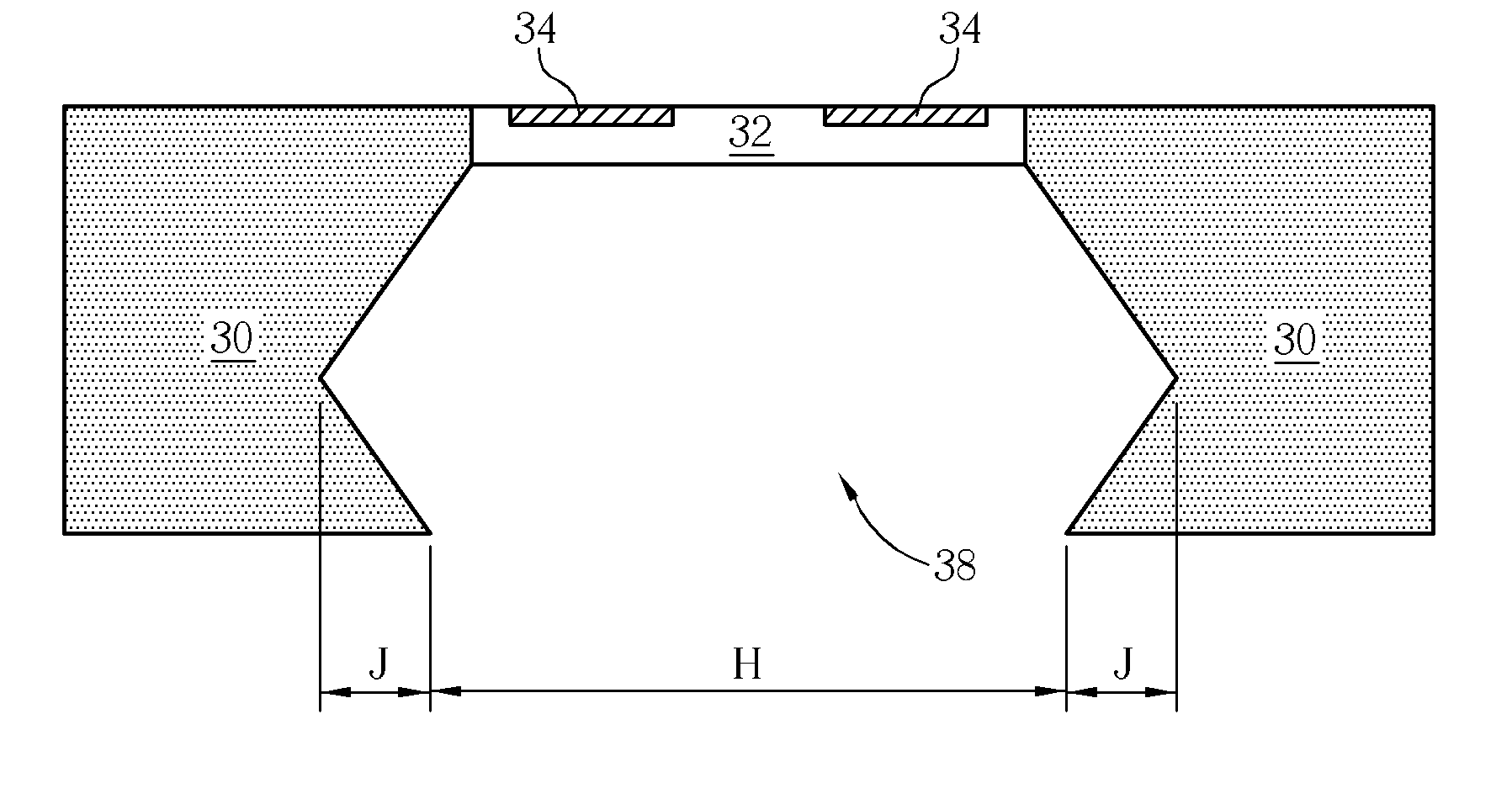
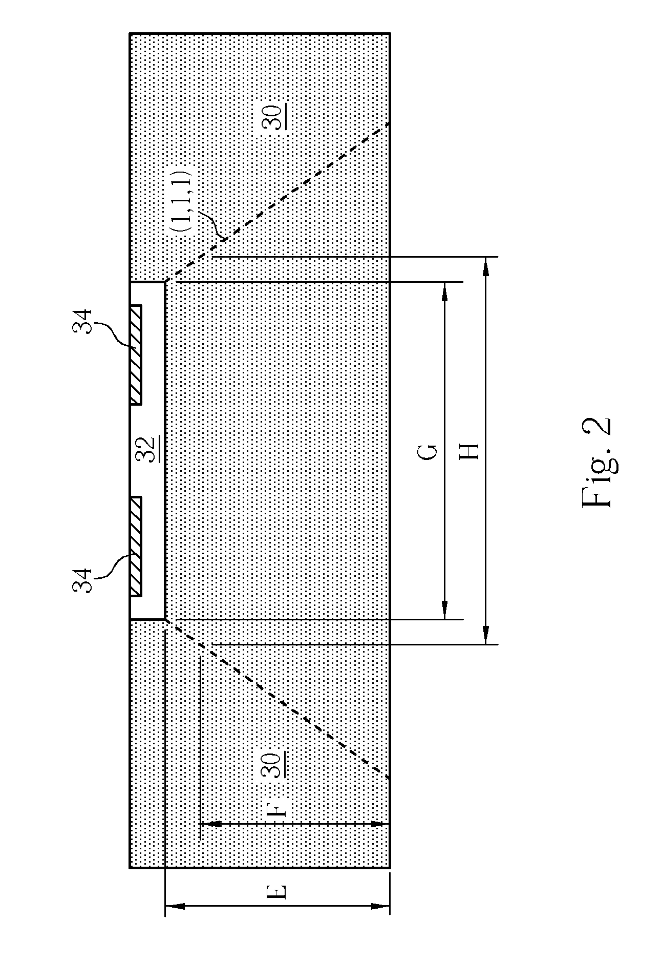
[0012] Refer to FIG. 2 to FIG. 5. FIG. 2 to FIG. 5 are schematic diagrams illustrating a method of reducing a dimension of a MEMS device according to a preferred embodiment of the present invention. According to the method of the present invention, the cavity of the MEMS device is accomplished by two-step etching, and only a single piezoresistive pressure sensor is illustrated for highlighting the feature of the present invention. As shown in FIG. 2, a single crystalline silicon substrate 30 e.g. a single crystalline silicon wafer is provided. The single crystalline silicon substrate 30 has a specific lattice orientation such as (1,0,0). The single crystalline silicon substrate 30 includes a diaphragm 32 disposed on the front surface, and a plurality of piezoresistors 34 formed in the diaphragm 32 to convert pressure signals into voltage signals. For a piezoresistive pressure sensor, the piezoresistors 34 are connected as a Wheaston bridge so as to amplify voltage signals.
[0013] Th...
PUM
 Abstract
Description
Claims
Application Information


