

Stack structure of carrier boards embedded with semiconductor components and method for fabricating the same
a carrier board and semiconductor technology, applied in the field of carrier board stack structure of carrier board embedded with semiconductor components, can solve the problems of less effect on the reduction of the area of the circuit board, large bulky packaging, and complex process for packaging, so as to simplify the semiconductor package process and reduce the manufacturing cost. , the effect of small capacity
- Summary
- Abstract
- Description
- Claims
- Application Information
AI Technical Summary
Benefits of technology
Problems solved by technology
Method used
Image

Examples
Embodiment Construction
[0022] The following illustrative embodiments are provided to illustrate the disclosure of the present invention, these and other advantages and effects can be apparently understood by those in the art after reading the disclosure of this specification. The present invention can also be performed or applied by other different embodiments. The details of the specification may be on the basis of different points and applications, and numerous modifications and variations can be devised without departing from the spirit of the present invention.
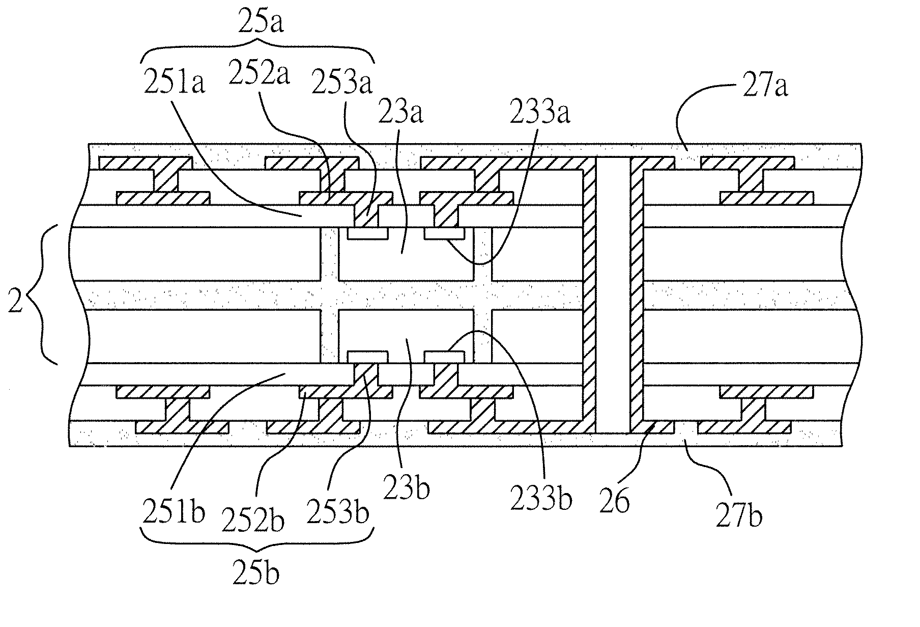
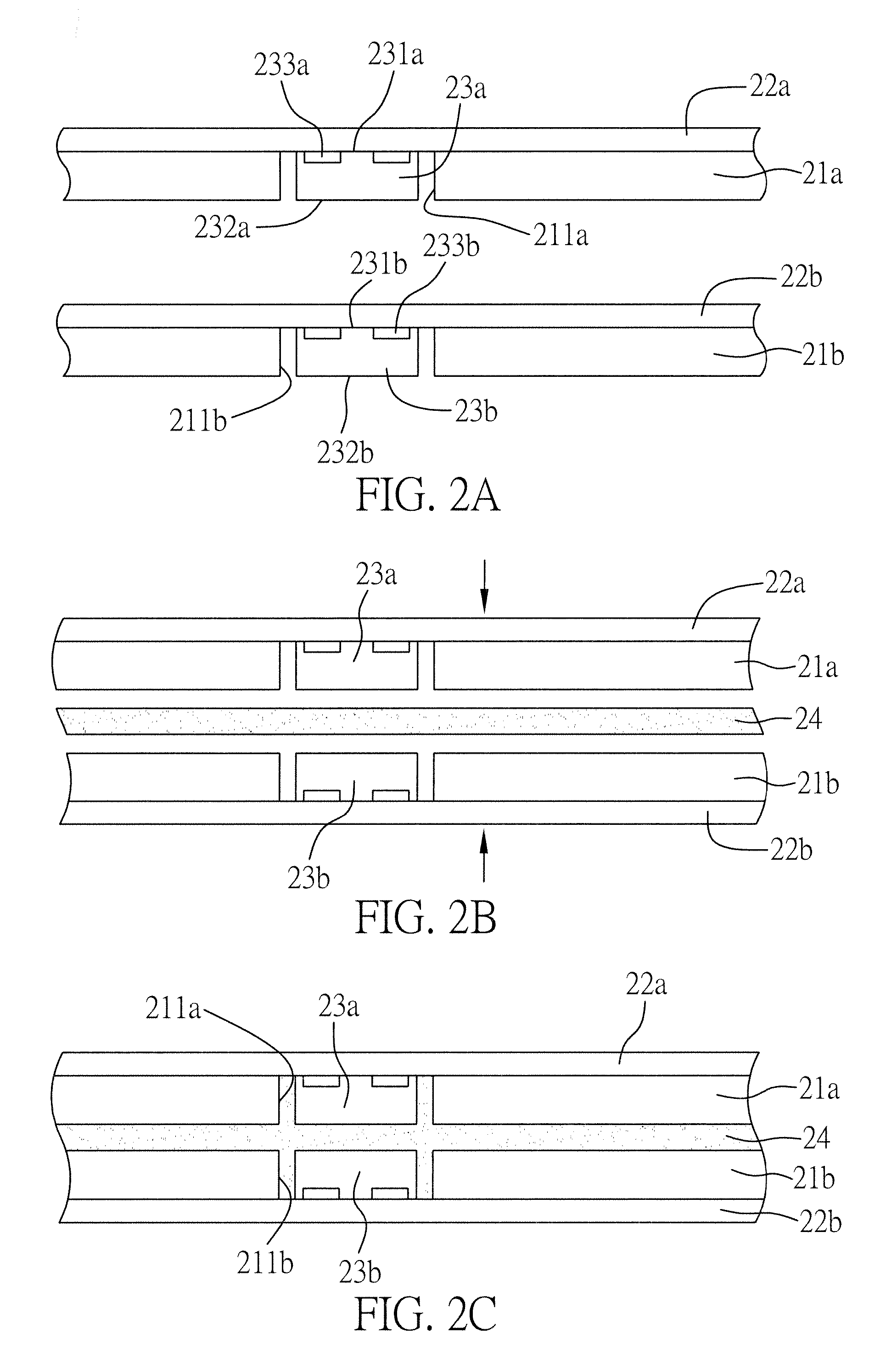
[0023]FIG. 2A through FIG. 2F are used to illustrate collectively a stack structure of carrier boards embedded with semiconductor components and a method for fabricating the same.
[0024] Please refer to FIG. 2A. The method forms a first through hole 211a in a first carrier board 21a, a second though hole 211b in a second carrier board 21b, a first protecting layer 22a on a surface of the first carrier board 21a for sealing one end of the first ...
PUM
 Abstract
Description
Claims
Application Information