Delayed locked loop circuit
a technology of delayed locking and loop circuit, which is applied in the direction of digital storage, pulse automatic control, instruments, etc., can solve the problems of time delay and power comsumption in the dll circuit, and achieve the effect of reducing power consumption in power-down mod
- Summary
- Abstract
- Description
- Claims
- Application Information
AI Technical Summary
Benefits of technology
Problems solved by technology
Method used
Image
Examples
Embodiment Construction
[0027] Hereinafter, a preferred embodiment of the present invention will be described in detail with reference to the accompanying drawings.
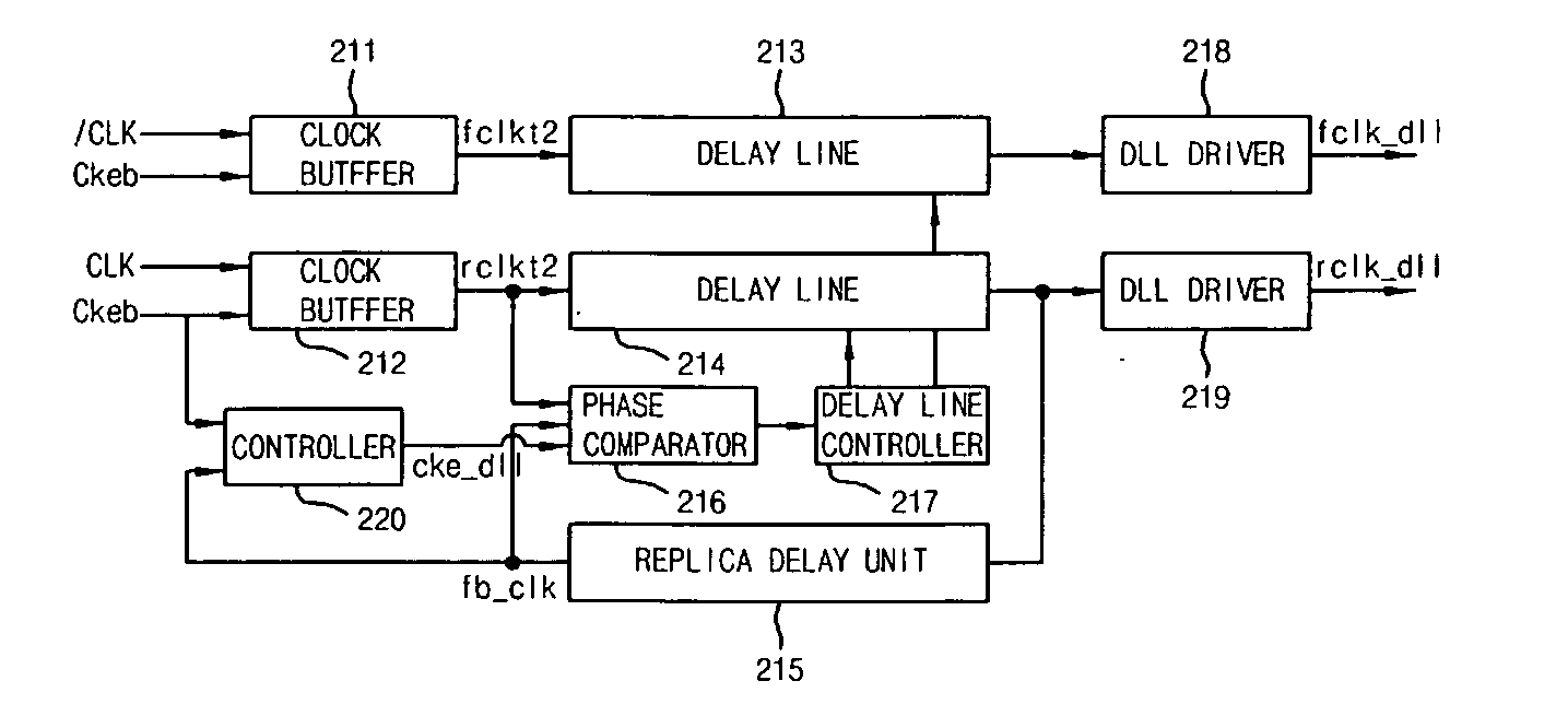
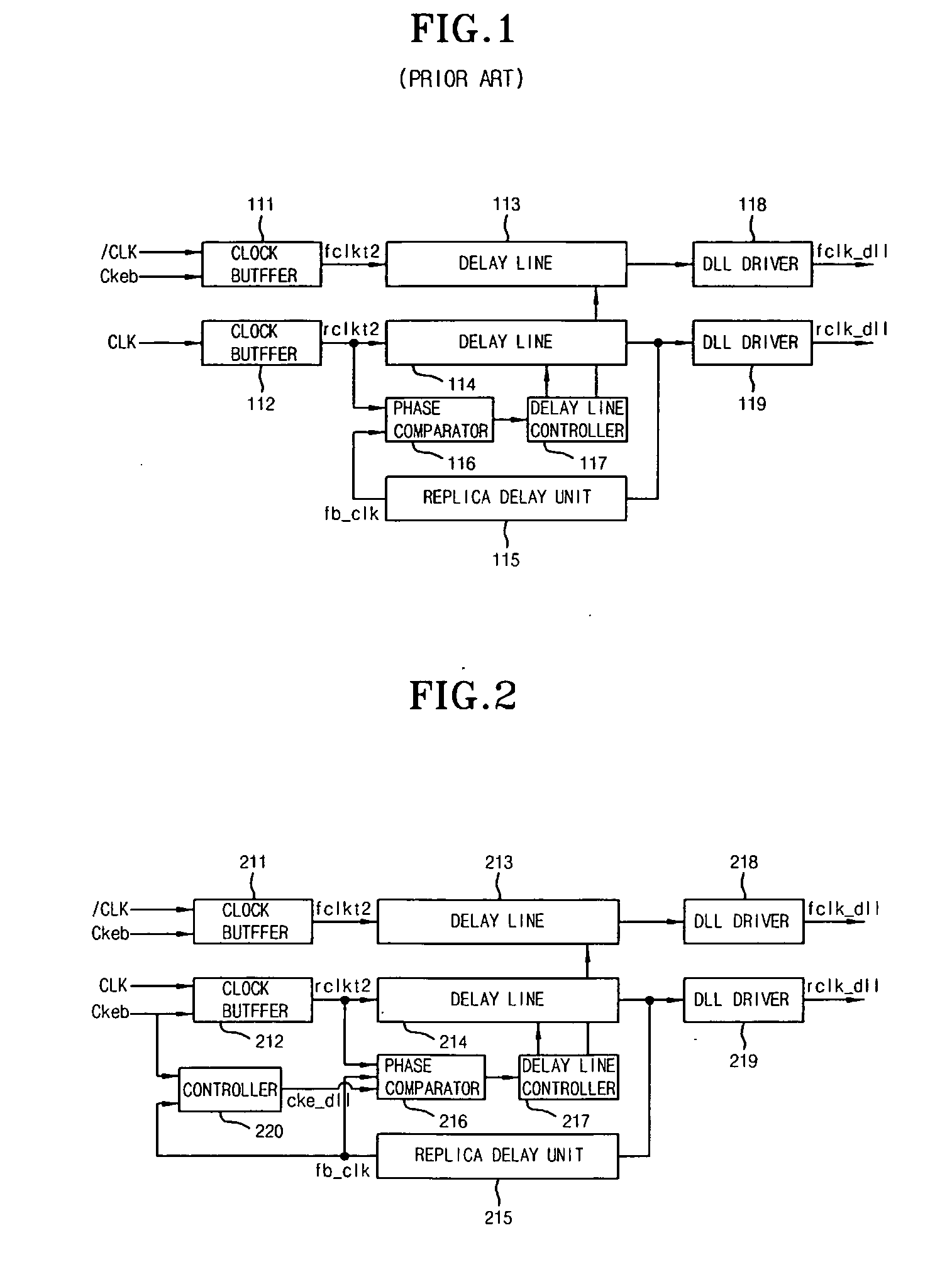
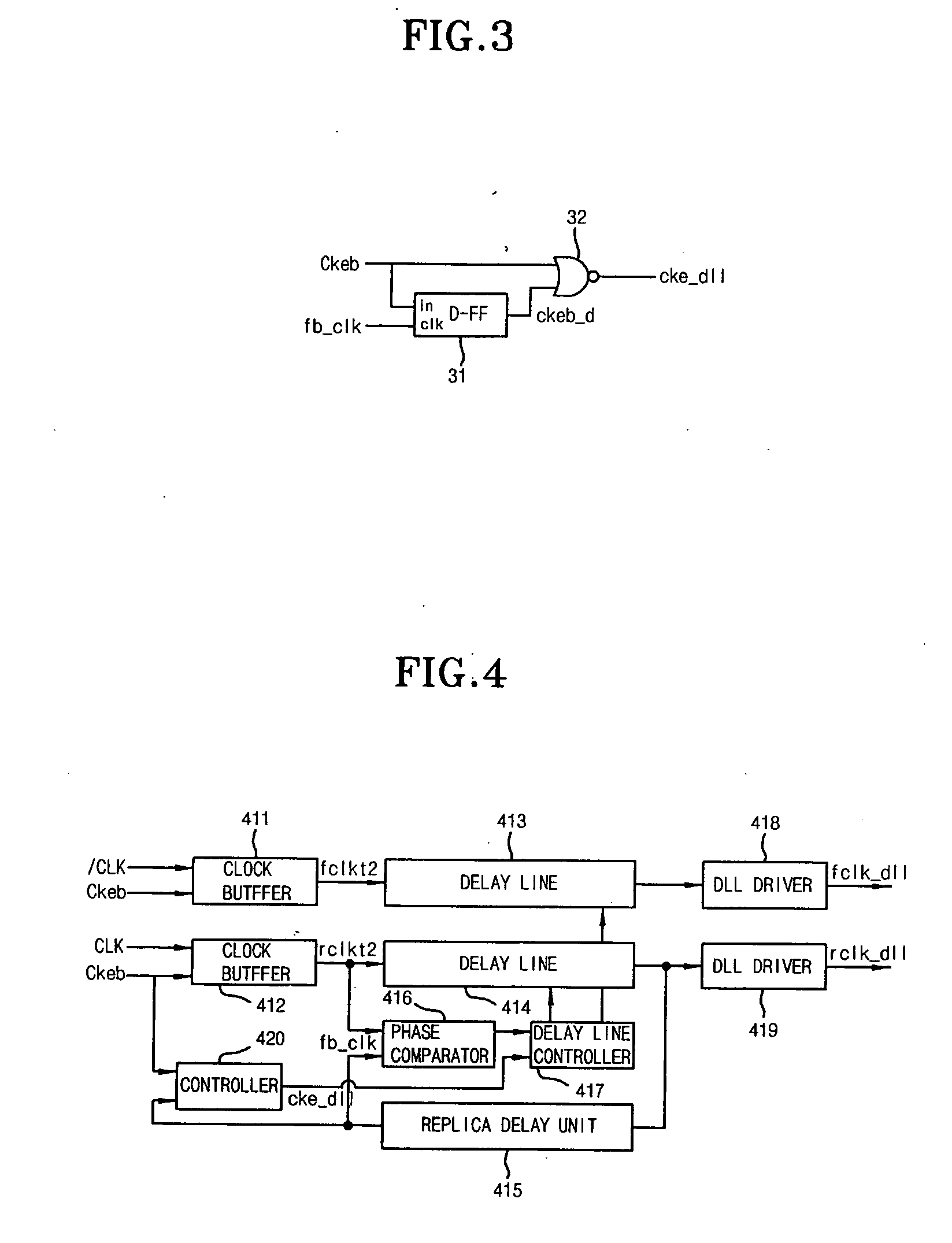
[0028]FIG. 2 is an embodiment of a DLL circuit according to the present invention. The clock buffers 211 and 212 are internal buffers that receive external clocks / CLK and CLK. The clock signal / CLK (pronounced as “clock bar” or as “clock complement”) is an inverted form of the clock signal, CLK. The clock signals / CLK and CLK, which have passed through the clock buffers 211 and 212 respectively, are indicated by internal clock signals fclkt2 and rclkt2. Unlike FIG. 1, it should be noted that the clock buffers 211 and 212 in FIG. 2 are controlled by an inverted signal Ckeb of a clock enable signal Cke. The signal Ckeb is a low level or logic zero when a memory device is in normal operation mode. The signal Ckeb is a high level or logic 1, when the memory device is in a power-down mode. For reference, the clock buffers 211 and 212 are disabled w...
PUM
 Abstract
Description
Claims
Application Information


