Analog-digital converter
- Summary
- Abstract
- Description
- Claims
- Application Information
AI Technical Summary
Benefits of technology
Problems solved by technology
Method used
Image

Examples
embodiment 1
[0044] (Circuitry)
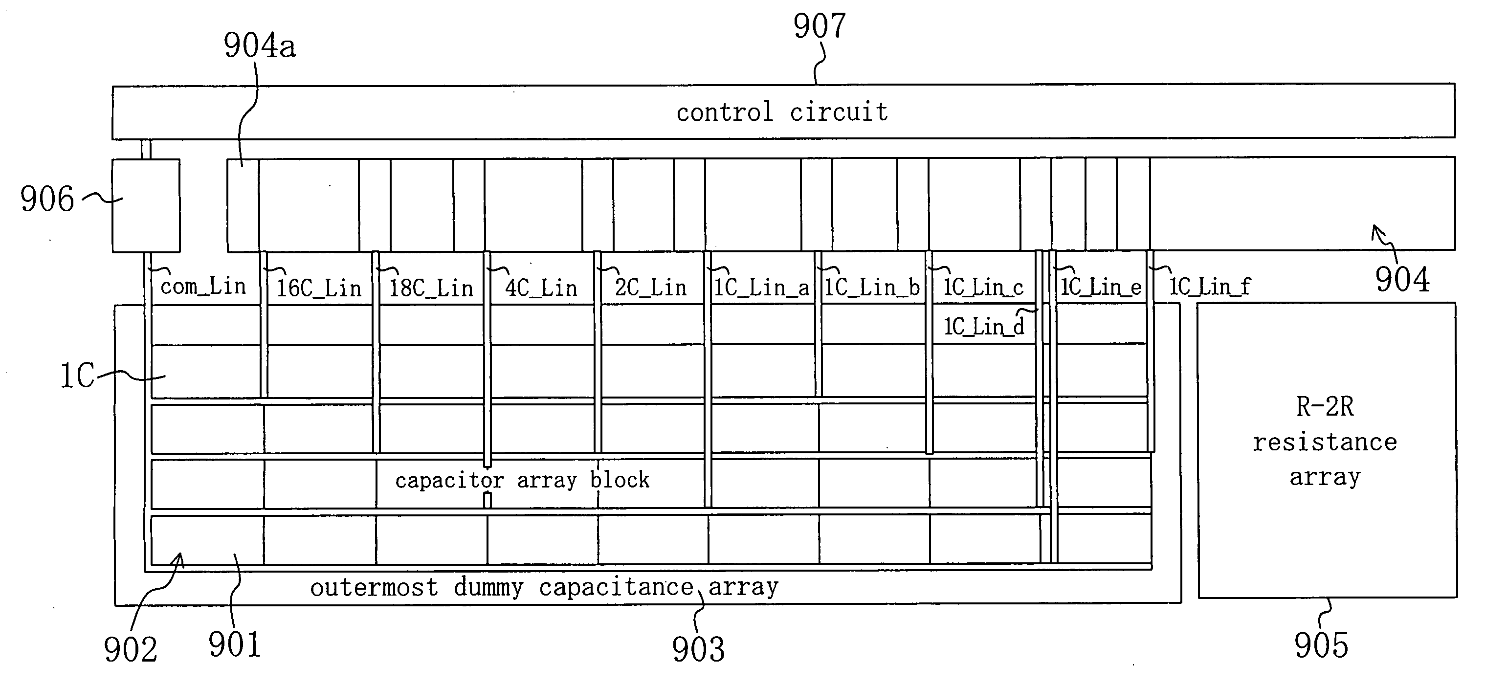
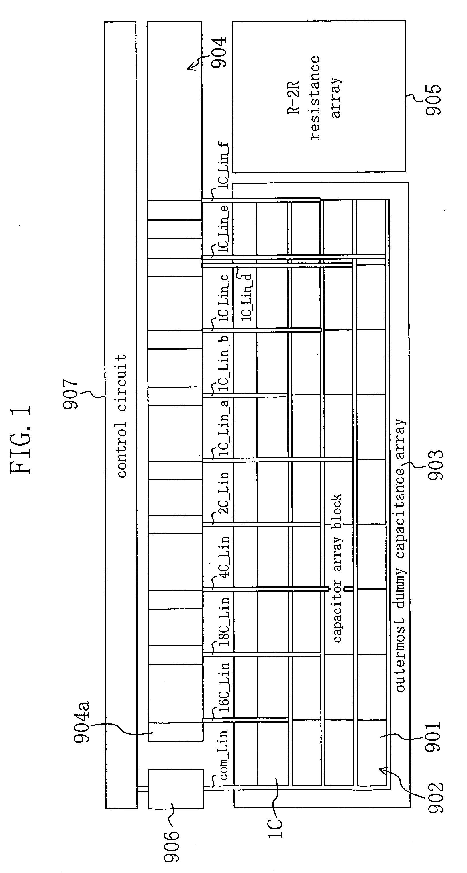
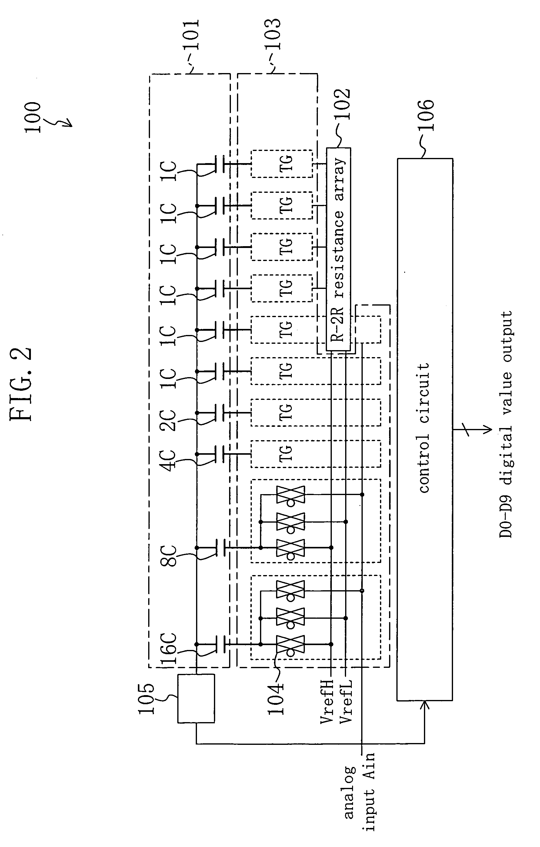
[0045] For an example of a 10-bit successive-approximation analog-digital converter according to Embodiment 1, a circuitry of an analog-digital converter 100 is first explained with reference to FIG. 2. This analog-digital converter 100 is provided with a capacitance array block 101 including capacitors 16C, 8C, 4C, 2C, and 1C having a capacitance ratio of 16:8:4:2:1. (Six capacitors 1C are provided and five of the six capacitors 1C serve as capacitances having capacitance ratios of 1 / 2, 1 / 4, 1 / 8, 1 / 16, and 1 / 32 by using an R-2R resistance array 102.)
[0046] The capacitors are connected to, for example, three analog switches 104 each provided in an analog switch group 103 at the electrodes on one side. These analog switches 104 selectively apply to each capacitor a high potential reference voltage VrefH, a low potential reference voltage VrefL, the high potential reference voltage VrefH and the low potential reference voltage VrefL divided by an R-2R resistance ar...
embodiment 2
[0062]FIGS. 11-13 show that the M2 layer 400 and the M3 layer 500 include dummy lines 411 and 511 extending lateral to the shields 403 and 404, and 503 and 504, respectively. These dummy lines 411 and 511 include portions which have the same width and pitch as the parallel portions 401a and 402a of the comb-shaped electrodes 401 and 402. This structure suppresses variations in the etching degree in a manufacturing process. Therefore, it is possible to easily increase the form accuracy in the parallel portions 401a and 402a, and accordingly, the accuracy in A / D conversion.
[0063] On the semiconductor substrate 200, the R-2R resistance array 102 and the control circuit 106, for example, are formed in a region which extends under the dummy lines 411 and 511 (or in a region including at least a part of the region which extends under the dummy lines 411 and 511). This makes it easy to further reduce the area consumed by the analog-digital converter over the semiconductor substrate.
[0064...
embodiment 3
[0065] As described in Embodiment 1, the M1 layer 300 is suitable to be used as the shields 313 and 323, because the use of the M1 layer 300 as the shields 313 and 323 easily reduces the effects of switching noise of the transistors 104a and 104b. However, the invention is not limited to this. The M1 layer 300 may also be used as an electrode of a capacitor in order to decrease the area or to increase the capacitance.
[0066] Specifically, in an example shown in FIG. 14 and FIG. 15, comb-shaped electrodes 351 and 352 are formed of the M1 layer 300. Similar to the comb-shaped electrodes 501 and 502, the comb-shaped electrodes 351 and 352 have parallel portions 351a and 352a and connection portions 351b and 352b. The comb-shaped electrodes 351 and 352 are respectively connected to the comb-shaped electrodes 401 and 402 of the M2 layer 400 via the contacts 409. The comb-shaped electrode 351 is formed such that the comb shaped electrode 402 extends over the comb-shaped electrode 351. The...
PUM
 Abstract
Description
Claims
Application Information
 - R&D Engineer
- R&D Manager
- IP Professional
- Industry Leading Data Capabilities
- Powerful AI technology
- Patent DNA Extraction
Browse by: Latest US Patents, China's latest patents, Technical Efficacy Thesaurus, Application Domain, Technology Topic.
© 2024 PatSnap. All rights reserved.Legal|Privacy policy|Modern Slavery Act Transparency Statement|Sitemap