Display device
- Summary
- Abstract
- Description
- Claims
- Application Information
AI Technical Summary
Benefits of technology
Problems solved by technology
Method used
Image

Examples
first embodiment
(First Embodiment)
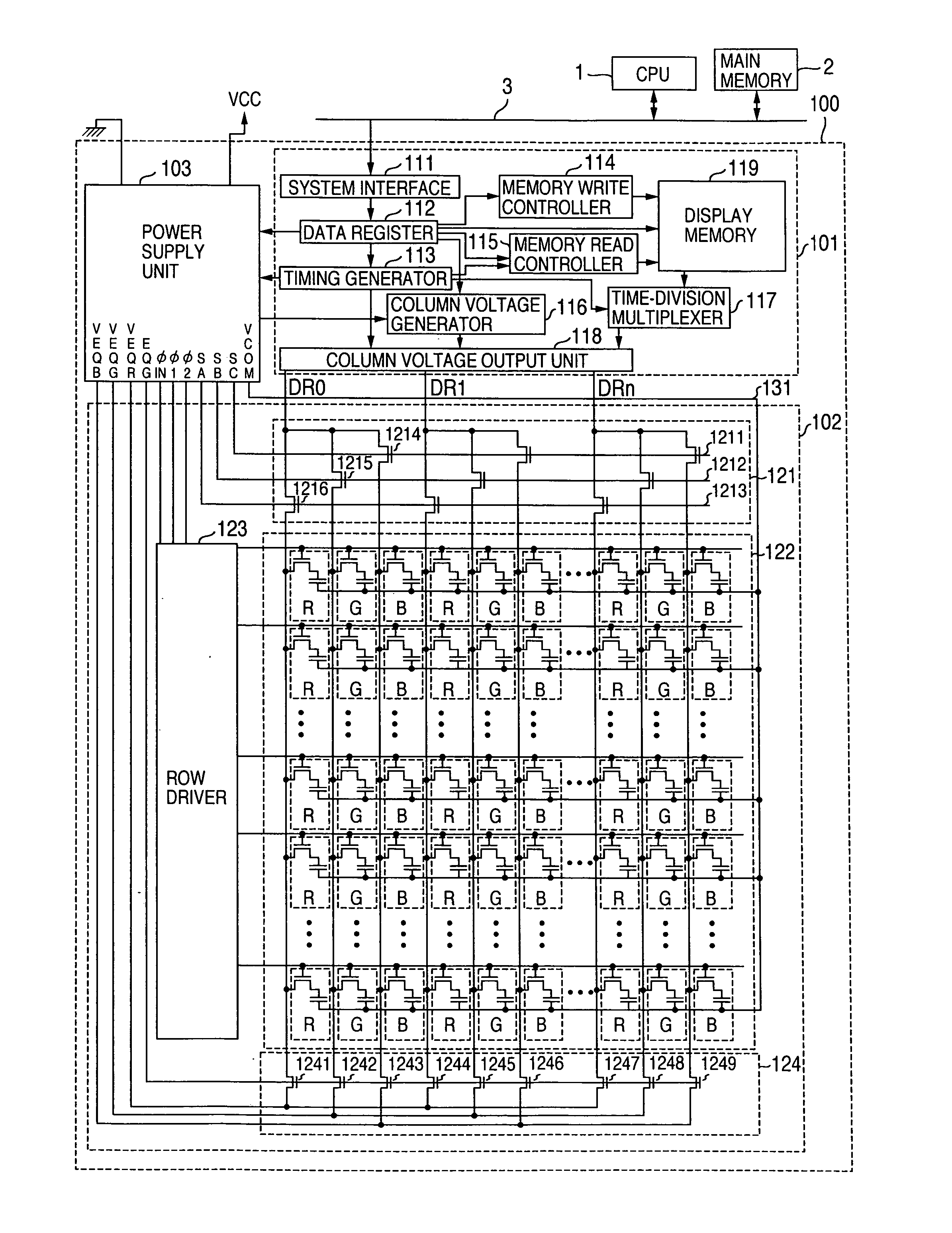
[0028] Hereafter, a first embodiment of the present invention will be described. FIG. 1 is a block diagram of a display device in the present embodiment. Reference numeral 100 denotes a display device, 101 a column driver, 102 a panel unit, and 103 a power supply unit.
[0029] In the column driver 101 shown in FIG. 1, reference numeral 111 denotes a system interface, 112 a data register, 113 a timing generator, 114 a memory write controller, 115 a memory card controller, 116 a column voltage generator, 117 a time-division multiplexer, 118 a column voltage output unit, and 119 a display memory.
[0030] In the panel unit 102 shown in FIG. 1, reference numeral 121 a distributor, 122 a pixel unit, 123 a row driver, and 124 an equalizer circuit. These are, for example, low temperature polysilicon TFT elements, and formed integrally on a glass substrate.
[0031] In the distributor 121 in this panel unit 102, reference numerals 1214, 1215 and 1216 denote TFT elements. In the...
second embodiment
(Second Embodiment)
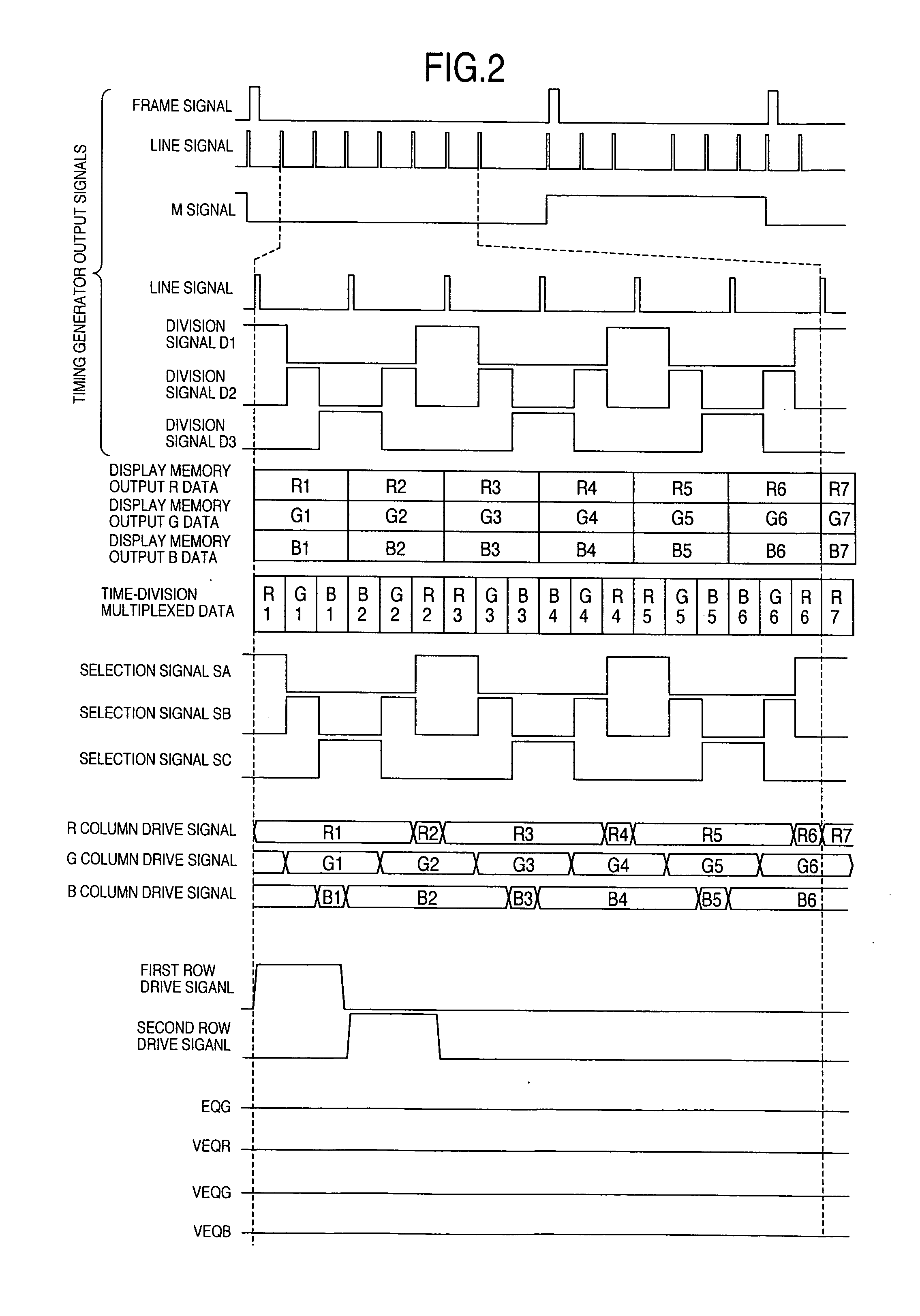
[0063] A second embodiment of the present invention will now be described with reference to FIGS. 1, 5, 6 and 7. The present embodiment differs from the first embodiment in that the order of time-division multiplexed data is definite as represented by RGB, RGB . . . as shown in FIG. 6 at the time of the ordinary operation. In addition, the present embodiment differs from the first embodiment in that line inversion is conducted, i.e., the potential level at the common electrode is inverted in phase every line at the time of the ordinary operation as shown in FIG. 6 and frame inversion is conducted, i.e., the potential level at the common electrode is inverted in phase every frame at the time of the partial display as shown in FIG. 7.
[0064]FIG. 1 was used in the description of the first embodiment. However, FIG. 1 is a block diagram which can be applied to the present embodiment as well. Unless otherwise stated in the ensuing description, each circuit has the same ...
third embodiment
(Third Embodiment)
[0080] A third embodiment of the present invention will now be described with reference to FIGS. 8, 9 and 10. The present embodiment differs from the first and second embodiments in that data corresponding to six columns are subjected to time-division multiplexing and input as the time-division multiplexed data and a column voltage on one wire is connected to six column electrodes via six distribution switches.
[0081]FIG. 8 is a block diagram of a display device in the present embodiment. In the distributor 121 on the liquid crystal panel unit 102, switch circuits 721, 722 and 723 for converting one signal supplied from the column voltage output unit 118 to six column drive signals are provided. Since these switch circuits have the same configuration, the switch circuit 721 will now be described as a representative one. One signal supplied from the column drive circuit 101 is connected to switches 701, 702, 703, 704, 705 and 706. These switches are switches which a...
PUM
 Abstract
Description
Claims
Application Information