Storage device, computer system, and data writing method

a technology of computer system and flash memory, applied in the direction of memory architecture accessing/allocation, instruments, sustainable buildings, etc., can solve the problems of no overwriting of data, disturbance to any not-selected cell, and low speed of flash memory, so as to reduce the frequency of data rewriting, increase the speed of writing to flash memory, and low standby power consumption

Inactive Publication Date: 2007-04-26
SONY CORP
View PDF6 Cites 26 Cited by
  • Summary
  • Abstract
  • Description
  • Claims
  • Application Information

AI Technical Summary

Benefits of technology

[0060] The invention enables to provide a small-capacity high-hit-rate low-access-overhead cache memory to a storage device with a main medium of flash memory, increase the speed of writing to a flash memory, and reduce th

Problems solved by technology

The concern here is that, as already mentioned above, the flash memories have a drawback of not being high in speed unless with the larger access unit.
Also with the fact that no overwriting of data is possible, rewriting always requires erasing with a much larger-sized erase block.
The erase uni

Method used


Image

  • Storage device, computer system, and data writing method
  • Storage device, computer system, and data writing method
  • Storage device, computer system, and data writing method

Examples


first embodiment

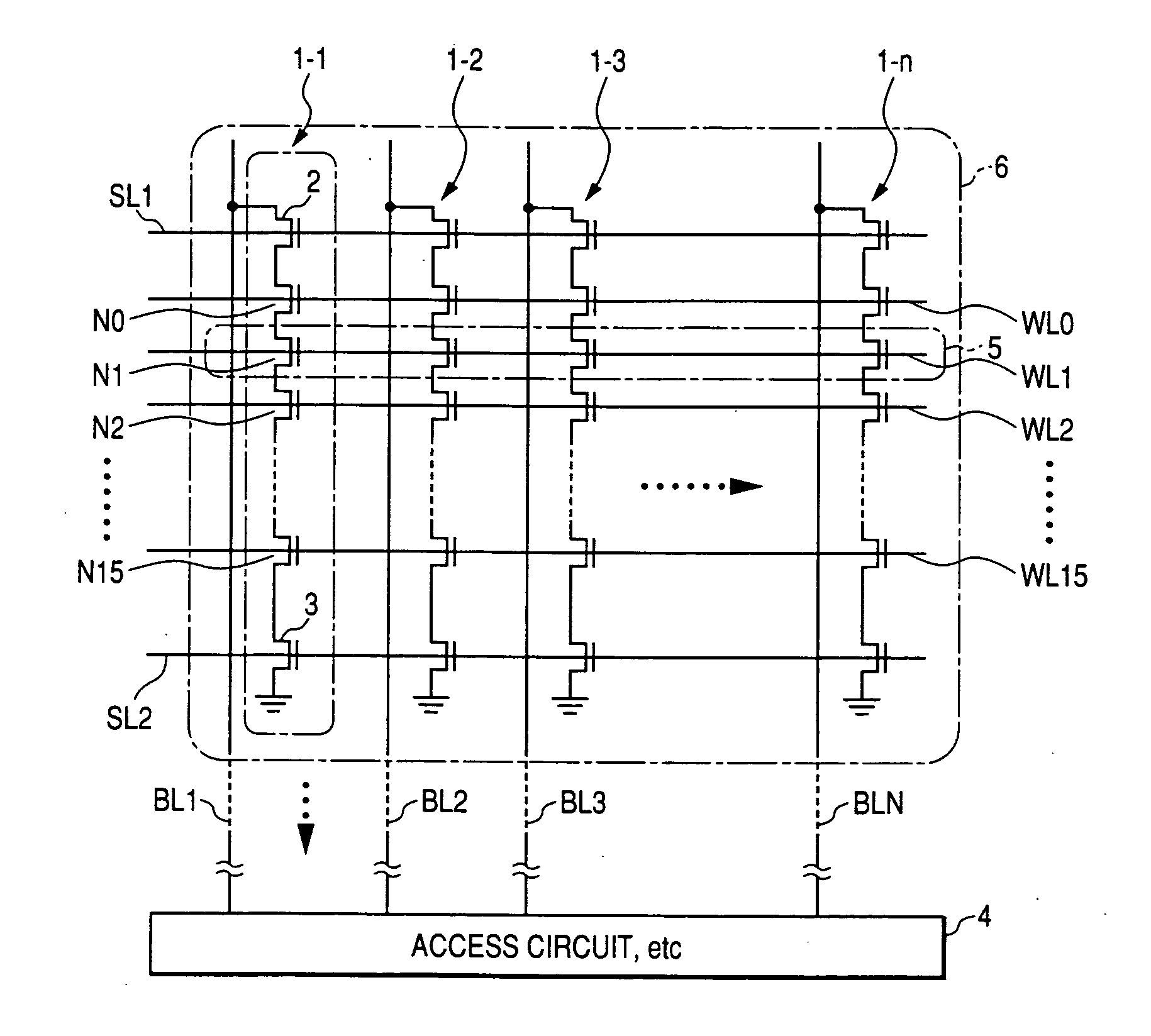
[0076]FIG. 3 is a diagram showing the configuration of a file storage device of the invention.

[0077] A file storage device 30 is configured to include an interface circuit (I / F) 31, a page buffer 32, a memory bus 33, a control circuit 34, NAND flash memories 35 and 36, a control circuit 37, a cache memory 38, and an internal bus 39. Reference numerals 40 to 43 each denote a page area, and the control circuit 34 includes an address conversion table 44, and a cache management table 45.

[0078] A flash memory device FLMD is formed by the components, e.g., the page buffer 32, the memory bus. 33, the NAND flash memories 35 and 36, the control circuit 37, and the internal bus 39.

[0079] In the file storage device 30, the 32-bit memory bus 33 is connected in parallel with the two-chip NAND flash memories 35 and 36 having an input / output of 16 bits. The two-chip NAND flash memories 35 and 36 are accessed simultaneously in parallel for data reading and writing.

[0080] The flash memories 35 an...

second embodiment

[0177] Described now is a second embodiment in which the invention is applied to such a case.

[0178]FIG. 7 is a diagram showing the configuration of a file storage device of the second embodiment of the invention.

[0179] A file storage device 30b is configured to include an interface circuit (I / F) 31b, a page buffer 32b, a memory bus 33b, a control circuit 34b, a NAND flash memories 35b and 36b, a control circuit 37b, a cache memory 38b, and an internal bus 39b. The control circuit 34b includes a cache management table 45b, and an erase block management table 46b.

[0180] The file storage device 30b of the second embodiment is of the configuration almost similar to that of the first embodiment, except that no address conversion is performed on a page unit basis.

[0181] In the file storage device 30b, the 32-bit memory bus 33b is connected in parallel with the two-chip NAND flash memories 35b and 36b having an input / output of 16 bits. The two-chip NAND flash memories 35b and 36b are ac...


PUM


Abstract

A storage device that includes: a flash memory device being a main storage medium; a cache memory for use for the flash memory device; and a control circuit. In the storage device, based on a write command and address information provided from outside, the control circuit selects either the flash memory device or the cache memory as a writing destination of input data.

Description

CROSS REFERENCES TO RELATED APPLICATIONS [0001] The present invention contains subject matter related to Japanese Patent Application JP 2005-305540 filed in the Japanese Patent Office on Oct. 20, 2005, the entire contents of which being incorporated herein by reference. BACKGROUND OF THE INVENTION [0002] 1. Field of the Invention [0003] The present invention relates to a storage device including a flash memory, a computer system using the storage device, and a data writing method and, more specifically, to a speed enhancement technology in the storage device for data transfer. [0004] 2. Description of the Related Art [0005] In recent years, flash memories are receiving attention as a storage medium for use for digital still cameras or mobile computer equipment. [0006] The flash memory is a semiconductor memory for storing therein data. For data storage, using electron tunneling or acceleration of hot electrons, electrons are injected to a floating gate or a trapping layer after bein...

Claims


Application Information

Patent Timeline
IPC IPC(8): G11C16/04
CPCG06F12/0888G06F12/0893G06F2212/2022Y02B60/1225G11C16/0483G11C16/12G06F2212/2024Y02D10/00
Inventor NISHIHARA, TOSHIYUKIYOSHIOKA, DAISUKA
Owner SONY CORP
Why Eureka
Try Eureka