

Vertical-cavity surface-emitting semiconductor laser device
- Summary
- Abstract
- Description
- Claims
- Application Information
AI Technical Summary
Benefits of technology
Problems solved by technology
Method used
Image

Examples
first embodiment
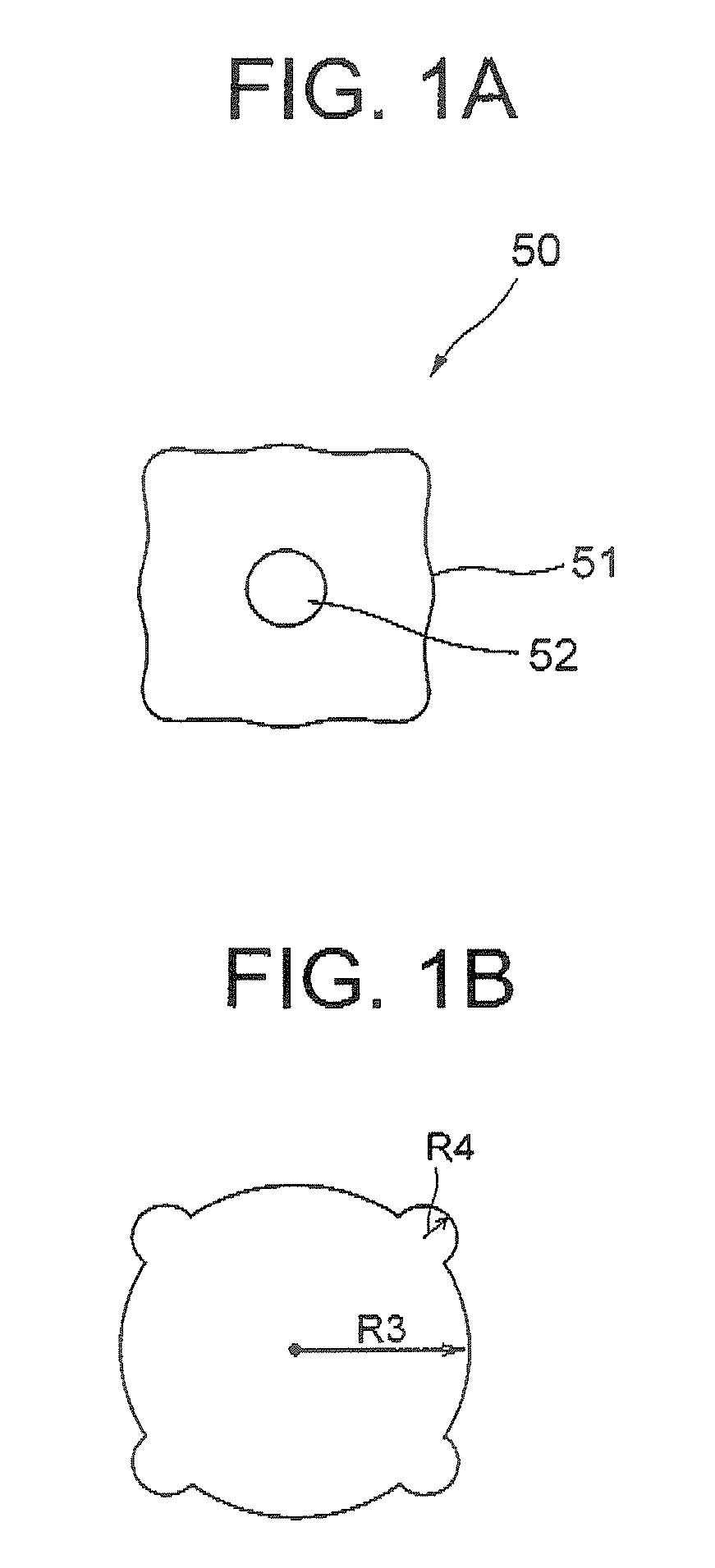
[0035] Now, the present invention is more specifically described with reference to accompanying drawings, wherein similar constituent elements are designated by similar or related reference numerals throughout the drawings. FIG. 1A shows a VCSEL device according to the present invention.
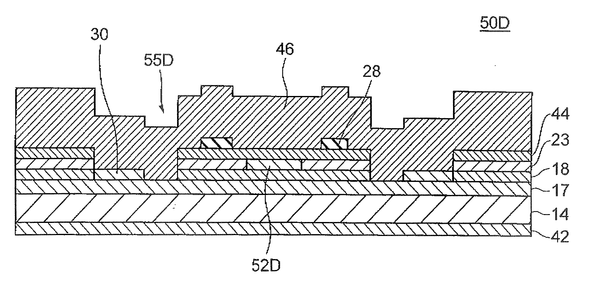
[0036] The VCSEL device, generally designated by numeral 50, according to the present embodiment is similar to the conventional VCSEL device 10 shown in FIG. 8 except for the planar shape of the mesa post 51, and for the shape of the current injection area 52 accordingly. More specifically, the VCSEL device 50 of the present embodiment has a layer structure similar to that of the VCSEL device of FIG. 8, and thus detailed description of the layer structure thereof will be omitted here for avoiding a duplication.
[0037] The VCSEL device 50 of the present embodiment includes the mesa post 51 having a cross-sectional structure wherein five circular arcs are combined together, differently from the rotatio...
second embodiment
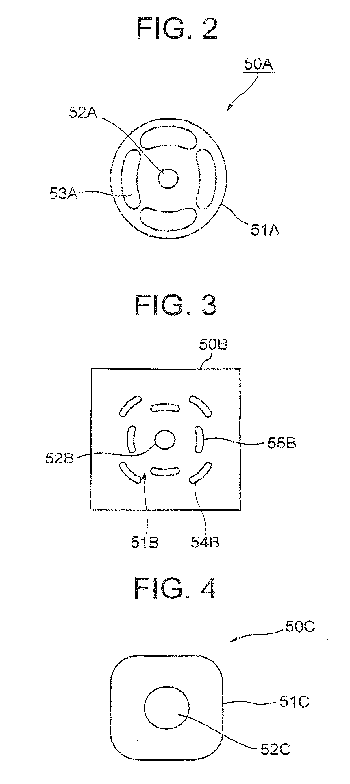
[0042]FIG. 2 shows the planar shape of the mesa post and current injection area of a VCSEL device according to the present invention. The VCSEL device, generally designated by reference sign 50A, according to the present embodiment includes four grooves 53A within the mesa post 51A in the vicinity of the cylindrical sidewall of the mesa post 51A. The four grooves 53A are arranged such that an annular grooves is separated in the vicinity of portions of the outer periphery of the mesa post 51A located in the direction to the (010), (01*0), (001) and (001*) crystal faces as viewed from the center of the mesa post 51A, and thus referred to as separate grooves hereinafter. The separate grooves 53A are filled with a polyimide film
[0043] In the configuration of the present embodiment, since the AlAs layer has an oxidation rate anisotropy in which the AlAs layer has a higher oxidation rate in the directions to the (010), (01*0), (001) and (001*) crystal faces, the AlAs layer has a longer di...
third embodiment
[0044]FIG. 3 shows a VCSEL device according to the present invention. The VCSEL device, generally designated by reference sign 50B, has eight separate grooves 541B, 55B outside the mesa post 51B, wherein the eight separate grooves 54B, 55B in combination correspond to the annular groove formed in the conventional VCSEL device. More specifically the inner periphery of the separate grooves 54B, 55B configure the sidewall of the mesa post 51B although the layer structure of the mesa post 51B is coupled to the layer structure of the peripheral area of the VCSEL device 50B via the locations at which the separate grooves 54B, 55B are separated from one another. Four separate grooves 54B located in the directions to the (010), (01*0), (001) and (001*) crystal faces as viewed from the center of the mesa post 51B are disposed radially outside of the location of the other four separate grooves 55B The inner periphery of the separate grooves 54B, 55B substantially configures the sidewall of th...
PUM
 Abstract
Description
Claims
Application Information