Eureka AIR delivers breakthrough ideas for toughest innovation challenges, trusted by R&D personnel around the world.

Three-dimensionally integrated electronic assembly

Inactive Publication Date: 2007-05-03
QIMONDA +1
View PDF10 Cites 21 Cited by
  • Summary
  • Abstract
  • Description
  • Claims
  • Application Information

AI Technical Summary

Benefits of technology

[0010] In one aspect, the invention specifies an arrangement for an integrated electronic assembly that results in a significant reduction of the mounting and packaging costs and of the area and space requirement in conjunction with a simultaneous reduction of the signal paths, flexible package pinout and 3-D integration.

Problems solved by technology

With advancing miniaturization, electronic assemblies are performing increasingly more complex functions.
It has been shown that considerable mounting and packaging costs arise in the case of integrated electronic assemblies, that is to say in the case of assemblies in which a plurality of different component and packaging types are combined with one another.
A specific problem on account of the continually increasing clock frequencies arises as a result of, in part, considerable signal paths or signal paths of different lengths with the associated signal propagation time differences or else the interference radiation.

Method used


Image

  • Three-dimensionally integrated electronic assembly
  • Three-dimensionally integrated electronic assembly
  • Three-dimensionally integrated electronic assembly

Examples


Embodiment Construction

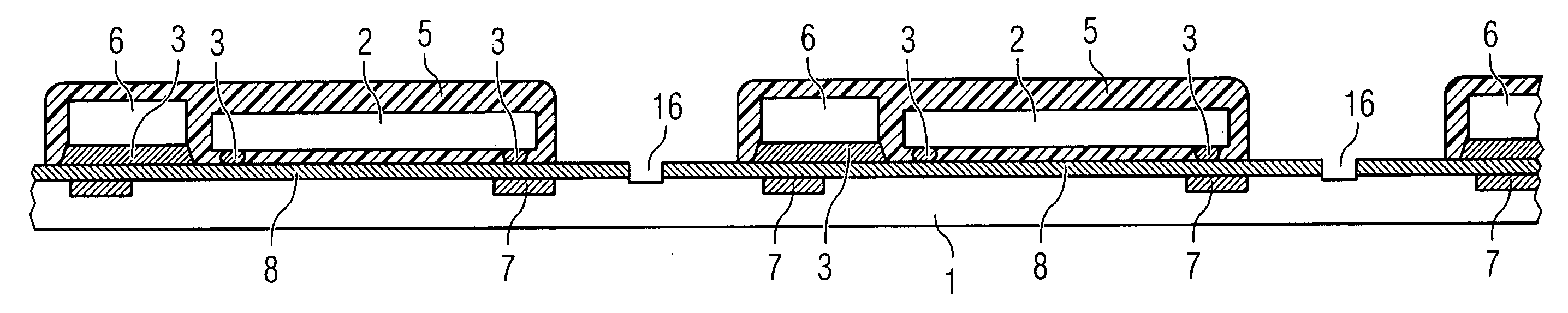
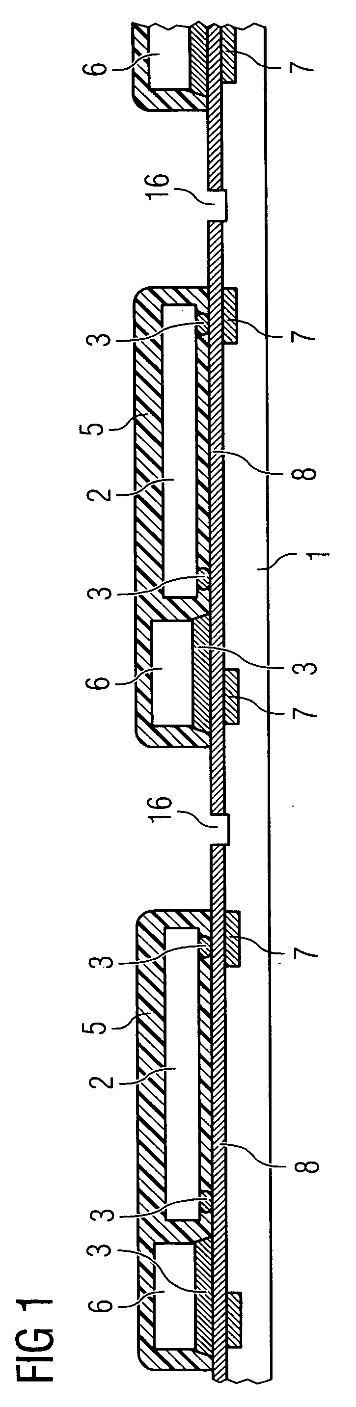
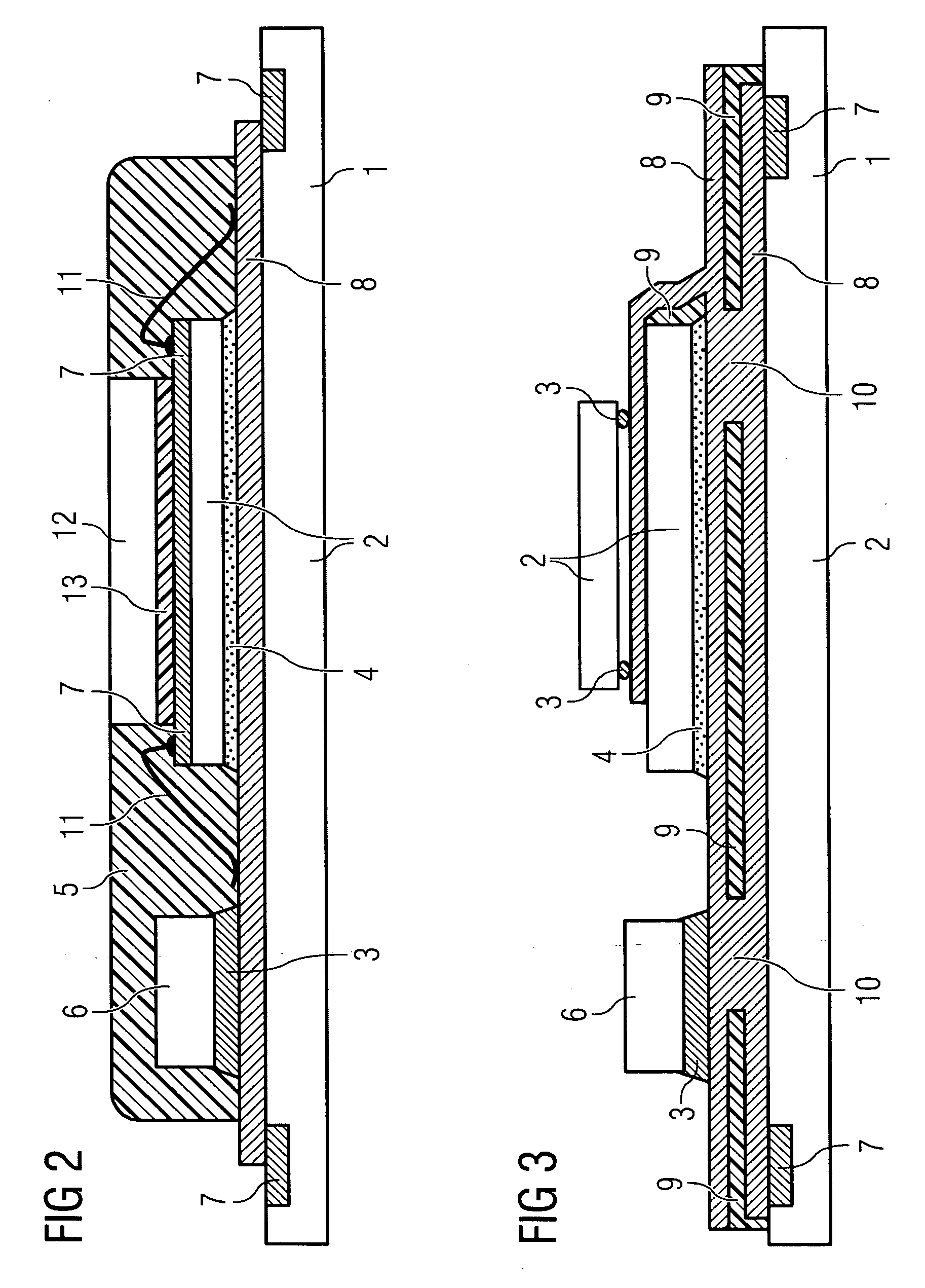
[0031]FIG. 1 shows a sectional illustration of a plurality of three-dimensionally integrated electronic assemblies that are arranged alongside one another on a wafer 1 (that is to say individual chips situated alongside one another, in each case, in the wafer assemblage), in the form of an excerpt. For the electrical contact-connection of further components, such as chips 2 and SMD components 6, an RDL 8 is situated on the wafer 1 and is electrically connected to the wafer 1 by means of bonding pads / contact areas 7. The chips 2 and SMD components 6 are, in each case, mounted on the RDL 8 by means of an electrical connection 3 (e.g., solder connection or adhesive-bonding connection).

[0032] The abbreviation RDL used here stands for redistribution lines, redistribution layer and / or other interconnects and areas for wiring, in each case comprising an insulator and interconnects. Furthermore, the term wafer is used for chips situated in the wafer assemblage.

[0033] Each electronic assem...


PUM


Abstract

A three-dimensionally integrated electronic assembly includes a substrate that includes active circuitry formed therein. At least one electronic component (e.g., an integrated circuit chip, active component, passive component, active assembly, and / or passive assembly) is mounted on the substrate. At least one redistribution connection is disposed between the substrate and at least one electronic component. Each electronic component is electrically coupled to the substrate and / or another electronic component mounted on the substrate by means of the redistribution connection.

Description

[0001] This application claims priority to German Patent Application 10 2005 041 452.4, which was filed Aug. 31, 2005 and is incorporated herein by reference. TECHNICAL FIELD [0002] The invention relates to a three-dimensionally integrated electronic assembly. BACKGROUND [0003] With advancing miniaturization, electronic assemblies are performing increasingly more complex functions. Typical areas of application are mobile radio devices, PDAs, cameras, clock computer and mobile data storage devices. In these devices it is typically necessary to integrate a plurality of chips, SMD (surface mount device) components and further elements in a small space. [0004] Chips and components are mounted, for example, on a PCB (printed circuit board), ceramic substrate or silicon substrate. Chips having a small area requirement for mounting can be fabricated as WLP (wafer level package). Multichip arrangements are produced as MCM (multi-chip module) in IC (integrated circuit) packages (e.g., SOP (s...

Claims


Application Information

Patent Timeline
IPC IPC(8): H01L29/00
CPCH01L23/147H01L23/36H01L23/5389H01L25/0657H01L25/16H01L25/162H01L2224/48091H01L2224/48145H01L2224/48227H01L2225/06506H01L2225/0651H01L2225/06513H01L2225/06517H01L2225/06582H01L2924/12044H01L2924/14H01L2924/19041H01L2924/30107H01L2924/3025H01L2924/00014H01L24/48H01L2924/12041H01L2924/00H01L2224/48465H01L2224/73265H01L2924/181H01L2924/1815H01L2224/16227H01L2224/32145H01L2224/73253H01L2924/19105H01L2924/00012H01L2224/45099H01L2224/45015H01L2924/207
Inventor ROEPER, HEIKOHANKOFER, JOHANNESHEDLER, HARRYKOHLHASE, ARMIN
Owner QIMONDA
Why Eureka
Eureka Blog
Learn More