High voltage charge pump with wide range of supply voltage

a high-voltage charge and supply voltage technology, applied in the field of high-voltage charge pumps, can solve the problems of circuits that do not work well at low supply voltage levels, require extra stages, and reduce the efficiency of circuits, so as to improve the efficiency of circuit design and layout, and reduce the effect of manufacturing process impa

Inactive Publication Date: 2007-05-03
BLUECHIPS TECH PTE
View PDF9 Cites 45 Cited by
  • Summary
  • Abstract
  • Description
  • Claims
  • Application Information

AI Technical Summary

Benefits of technology

[0065] Further, the charge pump of the present invention does not produce an output voltage that is higher than the desired output voltage and so does not require high breakdown voltage transistors, which have a negative impact on the manufacturing processes and, subsequently, cost. A charge pump according to the present invention is able to operate over a wider range of voltage input. Further, the current charge pump design may be easier to implement in design and layout because the charge pump can be divided into unit structures.
[0066] It is understood that a switc...

Problems solved by technology

Extra stages are required due to low efficiency of the circuit and an output voltage of at least one Vtm higher than the desired output voltage must be developed.
Furthermore, this circuit does not work well at low supply voltage levels.
However, it suffers a major loss in the output stage whereby the output voltage is at least one threshold drop from the desired value.
This means that high breakdown transistors are required which limit the flexibility of its application.
The complexity of the circuit adds unnecessary parasitic capacitance which degrades the charge pump efficiency.
To overcome this problem, long channel length must be used...

Method used


Image

  • High voltage charge pump with wide range of supply voltage
  • High voltage charge pump with wide range of supply voltage
  • High voltage charge pump with wide range of supply voltage

Examples


Embodiment Construction

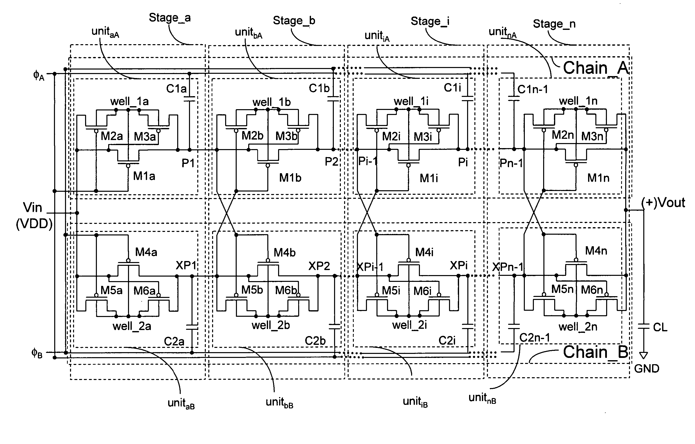
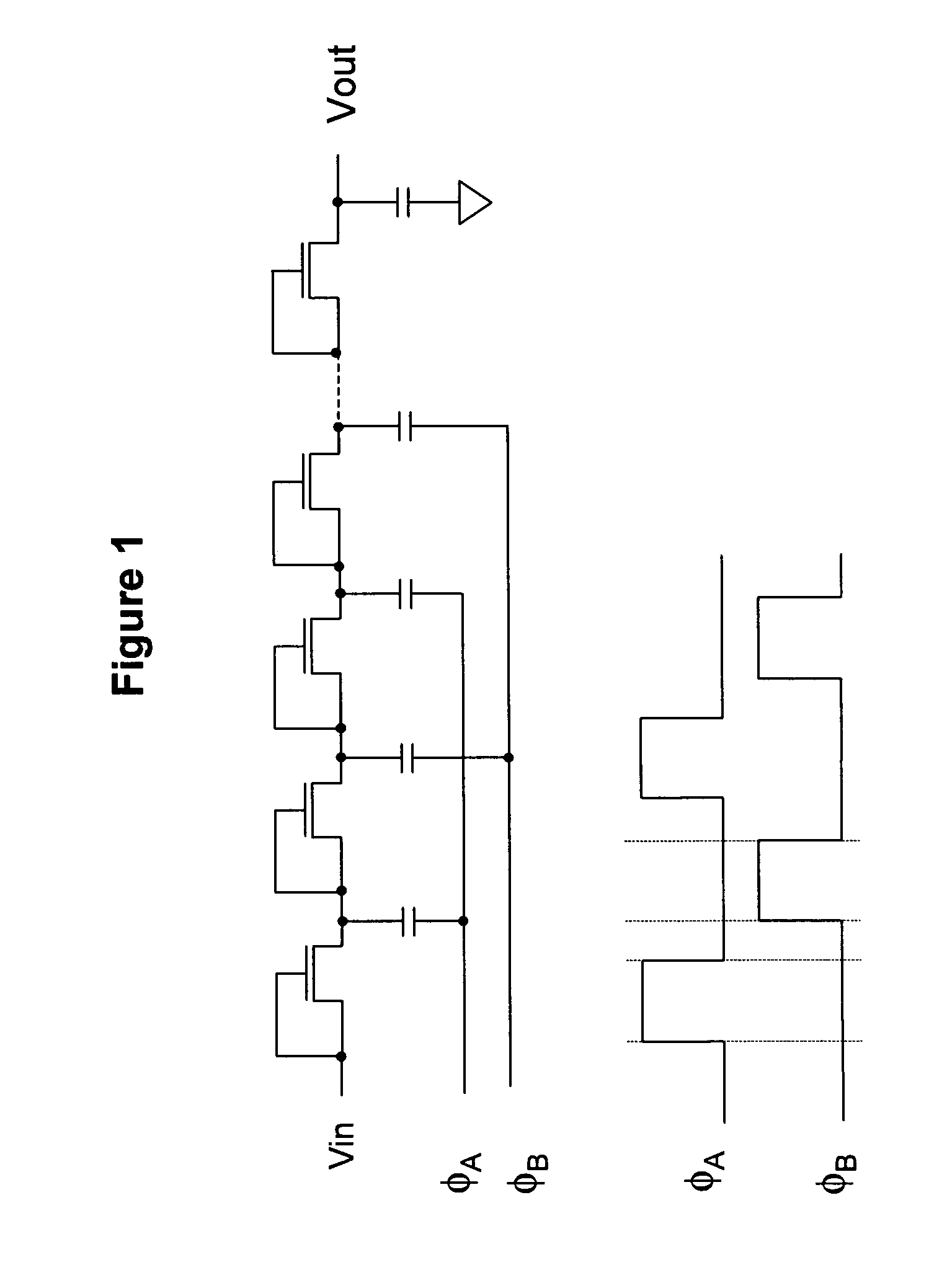
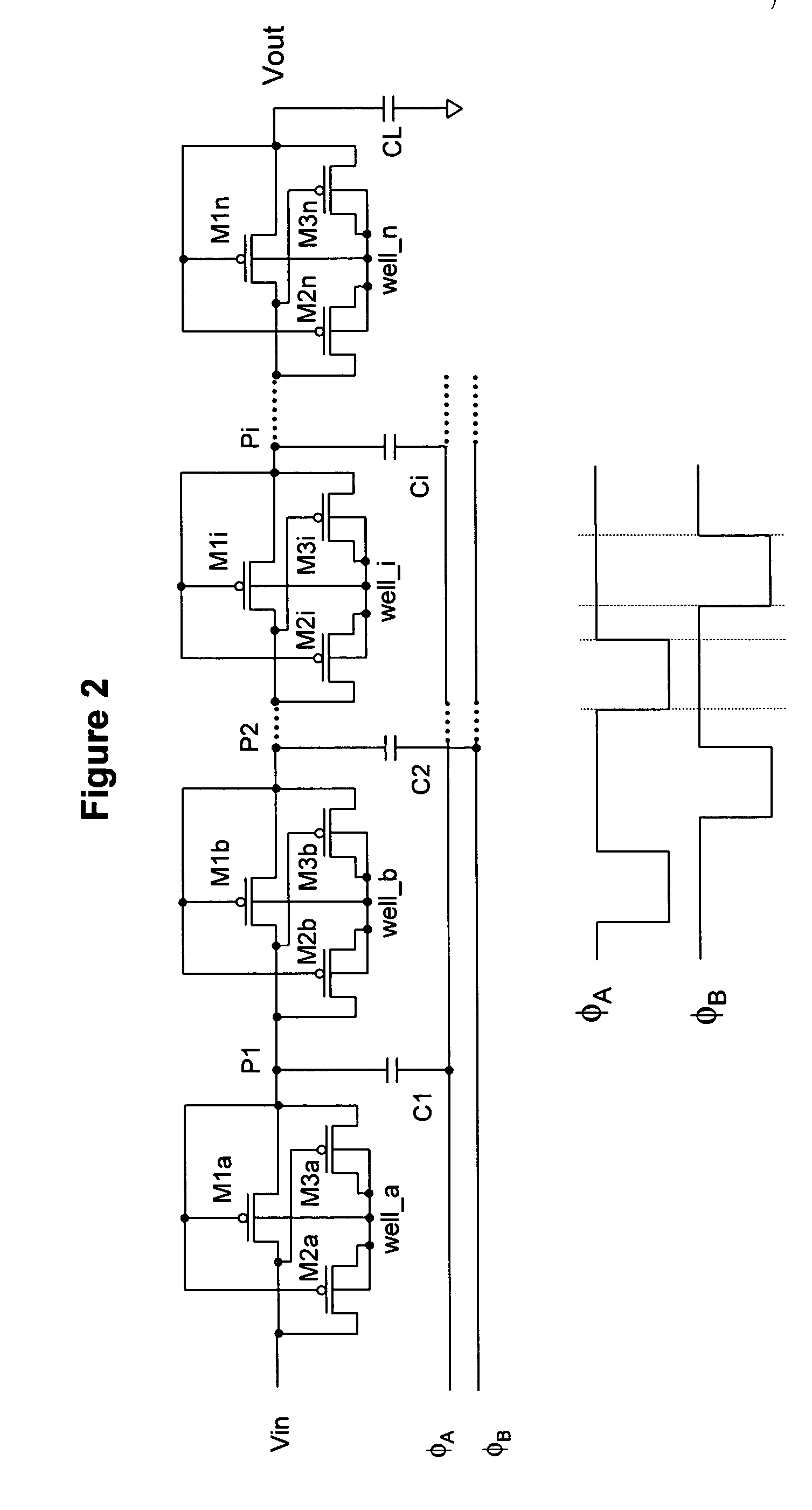
[0077] The electronic circuit diagram of the present example for a charge pump employing PMOS transistors configured as switches is shown in FIG. 3. Voltage signals for this circuit in FIG. 3 at various terminals are depicted in FIG. 4. As an example of using a plural number of charge transfer units, FIG. 5 presents a single charge transfer chain based on PMOS transistors. A further embodiment of the invention whereby the circuit uses NMOS transistors configured as switches, is shown in FIG. 6 with the voltage clock signals as presented in FIG. 7. All CMOS transistors employed according to the present invention (e.g., M1i, M2i, M3i, M4i, M5i & M6i), whether they are PMOS or NMOS transistors, are configured as switches.

[0078] The charge pump circuit according to FIG. 3 comprises charge transfer chains, chain_A and chain_B, enclosed by two separate dash-lines respectively. A plural number of charge transfer units (unitaA, unitbA, unitiA, . . . , unitnA) are serially connected to form...


PUM


Abstract

A charge pump circuit utilising CMOS or MOSFET (p-channel or n-channel) configured as switches for charge transfer is proposed. Instead of using the conventional diode-connected transistors, CMOS transistors configured as switches are used so that the threshold voltage drop across the stages of the charge pump is eliminated. Two of these charge pump chains are cross-coupled to bias each other at every stage. Consequently, the charge pump presented achieves higher voltage output efficiency with a wider supply voltage range.

Description

FIELD OF THE INVENTION [0001] The present invention relates to electronic devices used as charge pumps, and specifically high voltage charge pumps. In particular, it relates to architectures for a charge pump circuit to give higher output voltage than its input. BACKGROUND OF THE INVENTION [0002] Normally, high voltage charge pumps are circuits that pump electric charges into capacitors for generating a positive or negative output voltage higher than the supply. High voltage charge pumps are commonly used for providing high voltages to programme / erase programmable ROM (Read Only Memory) elements, such as EEPROM (Electrically Erasable and Programmable Read Only Memory), flash memory, power solid-state particles detectors and photo-multipliers, drive analogue switches, etc. Conventional charge pump circuits include a number of serially connected charge transfer stages and they are driven by clock signals. Every charge transfer stage comprises a diode (or transistor configured as a dio...

Claims


Application Information

Patent Timeline
IPC IPC(8): G05F1/10
CPCH02M3/07
Inventor FIRMANSYAH, TEEZAR R.NG, GEK Y.
Owner BLUECHIPS TECH PTE
Why Eureka
Try Eureka