Optical logic element

Inactive Publication Date: 2007-05-03
SAMSUNG ELECTRONICS CO LTD +1
View PDF6 Cites 2 Cited by
  • Summary
  • Abstract
  • Description
  • Claims
  • Application Information

AI Technical Summary

Benefits of technology

[0010] It is therefore a feature of an embodiment of the present invention to provide an all optical logic element that can realize a NOR circuit.
[0011] It is therefore another feature of an embodiment of the present invention to provide an all optical logic element that can realize a NAND circuit.
[0012] It is yet another feature of an embodiment of the present invention to provide an all optical logic element that can realize XOR, NOR, OR and NAND circuits.
[0017] When the power of the first optical signal is at a high level, the first optical amplifier may delay the phase of the continuous optical signal by π, when the power of the first optical signal is at a low level, the first optical amplifier may not delay the phase of the continuous optical signal, when the power of the second optical signal is at a high level, the second optical amplifier may delay the phase of the continuous optical signal by π, when the power of the second optical signal is at a low level, the second optical amplifier may not delay the phase of the continuous optical signal the first phase shifter shifts the phase of an output of the first optical amplifier by (2n+1)π, where n is an integer, a high level gain of the first optical amplifier may be equal to a high level gain of the second optical amplifier, and a low level gain of the first optical amplifier may be equal to a low level gain of the second optical amplifier.

Problems solved by technology

However, XGM may result in a low extinction ratio and a low signal quality.
Thus, this method may not be appropriate for high speed operation.

Method used


Image

  • Optical logic element
  • Optical logic element
  • Optical logic element

Examples


Embodiment Construction

[0034] Korean Patent Application No.10-2005-0099942, filed on Oct. 22, 2005, in the Korean Intellectual Property Office, and entitled: “Optical Logic Element,” is incorporated by reference herein in its entirety.

[0035] The present invention will now be described more fully hereinafter with reference to the accompanying drawings, in which exemplary embodiments of the invention are illustrated. The invention may, however, be embodied in different forms and should not be construed as limited to the embodiments set forth herein. Rather, these embodiments are provided so that this disclosure will be thorough and complete, and will fully convey the scope of the invention to those skilled in the art.

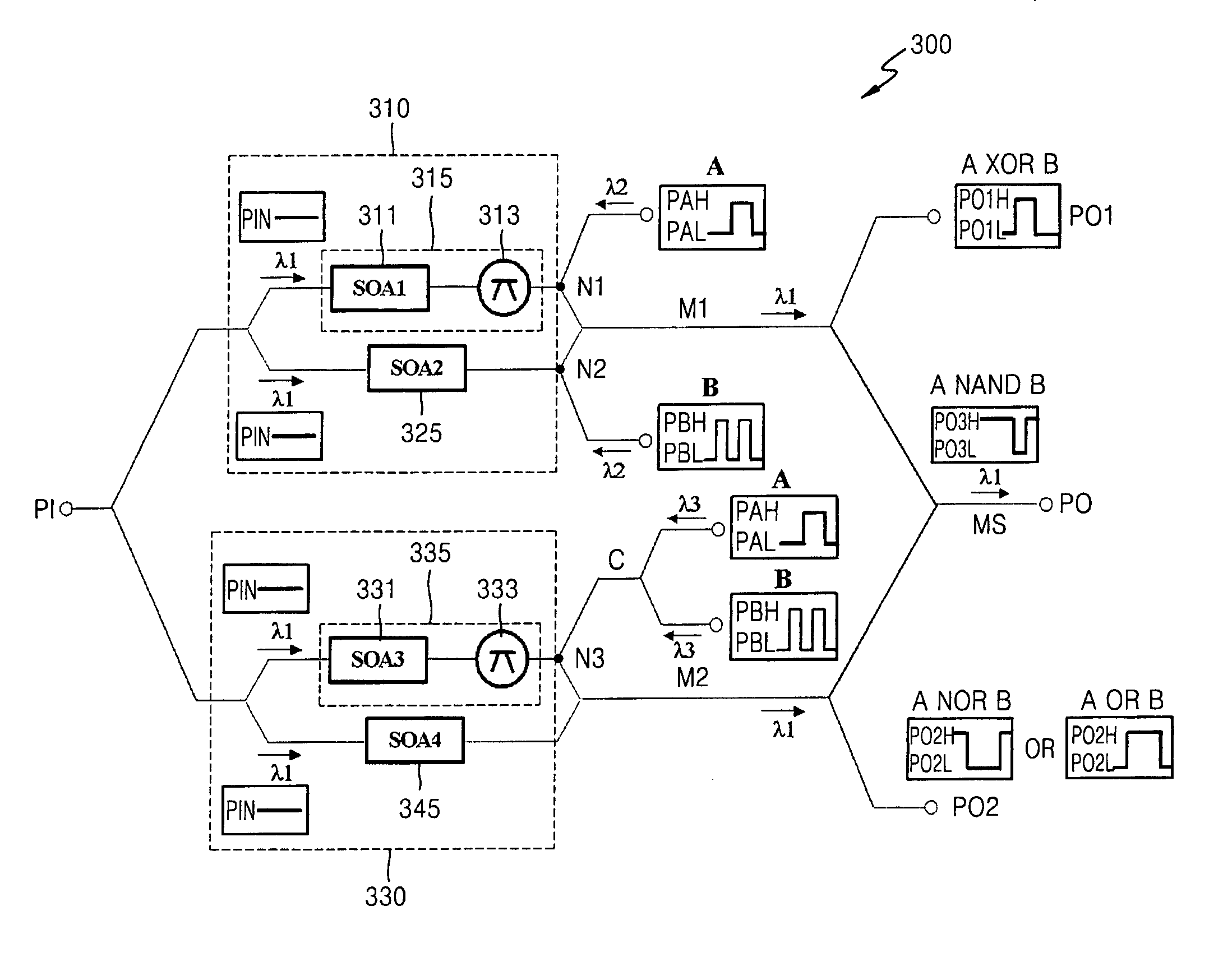
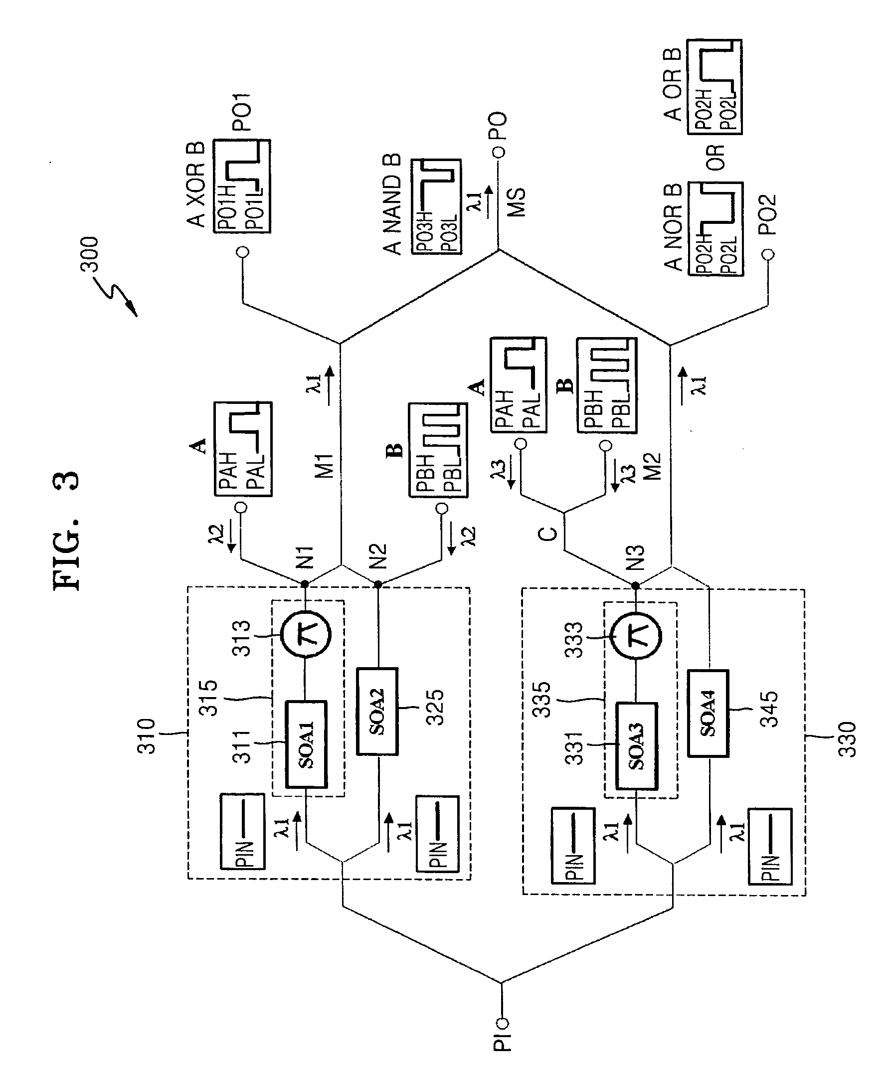
[0036] In accordance with embodiments of the present invention, an optical logic element may be realized using all-optical XOR, NOR, OR, and NAND circuits. As a result, any desired optical logic element may be readily constructed.

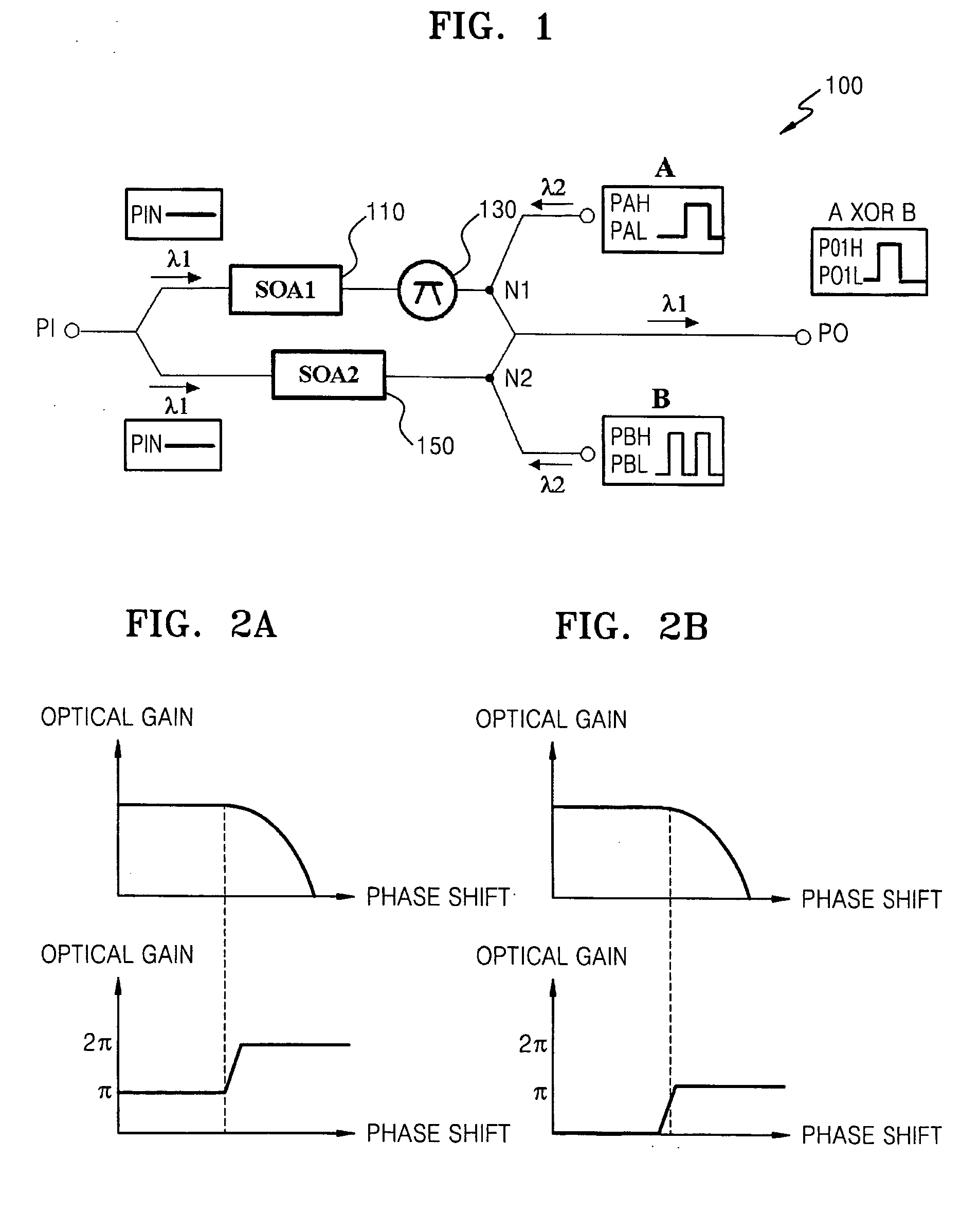
[0037]FIG. 1 illustrates a schematic diagram of an XOR circuit...


PUM


Abstract

An optical logic element includes a first interferometer modulating a continuous optical signal in response to first and second optical signals to output a first modulation signal, and a second interferometer modulating the continuous optical signal in response to a sum signal equal to the sum of the first and second optical signals to output a second modulation signal. The first and second modulation signals and the sum signal are respectively the results of predetermined logic operations performed on the first and second optical signals.

Description

BACKGROUND OF THE INVENTION [0001] 1. Field of the Invention [0002] The present invention relates to an optical logic element. More particularly, the present invention relates to an optical logic element using an interferometer realized using a semiconductor optical amplifier (SOA). [0003] 2. Description of the Related Art [0004] Forming an ultrahigh optical communication network may include facilitating networking functions, e.g., switching, signal re-generating, addressing, header identifying, data encoding and encrypting, pattern matching, and the like. Also, an optical logic element, i.e., an all-optical logic gate, may be required to realize optical communication networking functions. [0005] SOAs are widely used to realize all-optical logic gates used in optical communications. A non-linear optical phenomenon, e.g., cross gain modulation (XGM), cross phase modulation (XPM), cross polarization modulation (XPoIM), four wave mixing (FWM), or the like, may occur in such an SOA. All...

Claims


Application Information

Patent Timeline
IPC IPC(8): H04B10/04
CPCG02F3/00G02F2002/006G02F2/006H03K19/14
Inventor KIM, JOO-YOUPHAN, SANG-KOOK
Owner SAMSUNG ELECTRONICS CO LTD
Why Eureka
Try Eureka