Plasma for patterning advanced gate stacks

a technology of advanced gate stacks and plasma, which is applied in the direction of basic electric elements, semiconductor/solid-state device manufacturing, electrical equipment, etc., can solve the problems of incompatibility of stack materials, gate profiles that cannot be re-arranged, and none of them can achieve the effect of preserving the vertical profile of the gate stack after patterning

Inactive Publication Date: 2007-05-03
INTERUNIVERSITAIR MICRO ELECTRONICS CENT (IMEC VZW)
View PDF8 Cites 202 Cited by
  • Summary
  • Abstract
  • Description
  • Claims
  • Application Information

AI Technical Summary

Benefits of technology

[0006] A dry-etch plasma composition for preserving the vertical profile of a structu

Problems solved by technology

The key challenge is to adapt the conventional gate etch process flow to the metal gate stack.
Etching of metal gates has been studied addressing metal gate and gate oxide surface roughness, CD control, etch selectivity, and low damage etching but none of them succeeded in

Method used


Image

  • Plasma for patterning advanced gate stacks
  • Plasma for patterning advanced gate stacks
  • Plasma for patterning advanced gate stacks

Examples


example 1

Application of BCl3 / N2 Plasma for TaN Gate Profile Control

[0093] The BCl3 / N2 plasma was used to etch TaN metal gates, in the example presented here said TaN metal gate is present in a TiN / TaN gate stack where 15 nm TaN is in the contact with the gate dielectric and 70 nm TiN covers the TaN or in other words 70 nm TiN is situated on top of said 15 nm TaN.

[0094] The most critical step is TaN etching after TiN patterning. BCl3 plasma is used here for the TaN patterning as it is selective to the Si substrate and can be used as high-k removal as well.

[0095] If TaN is etched with pure BCl3 plasma, then a notch (lateral attack) is observed in the TaN layer.

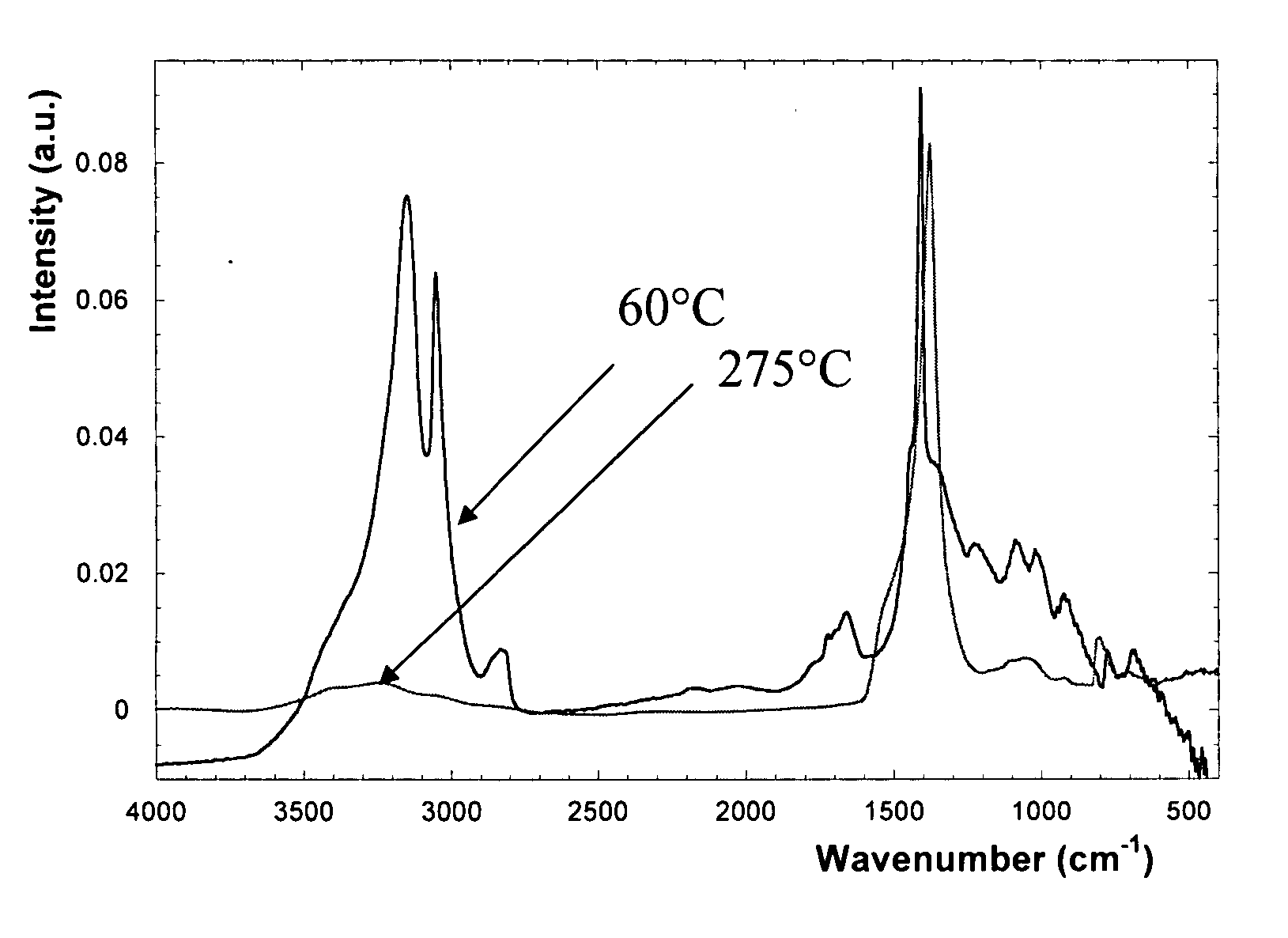
[0096]FIG. 4A shows the gate profile after etching in pure BCl3, an arrow indicates the lateral attack of TaN.

[0097] The addition of 5% of N2 to the BCl3 plasma resulted in a straight TaN profile without the lateral attack of the TaN layer.

[0098] The effect of N2 addition is illustrated in FIG. 4B. A BxNy comprising passivation lay...

example 2

Application of BCl3 / N2 Plasma for Pure Ge Gate Profile Control

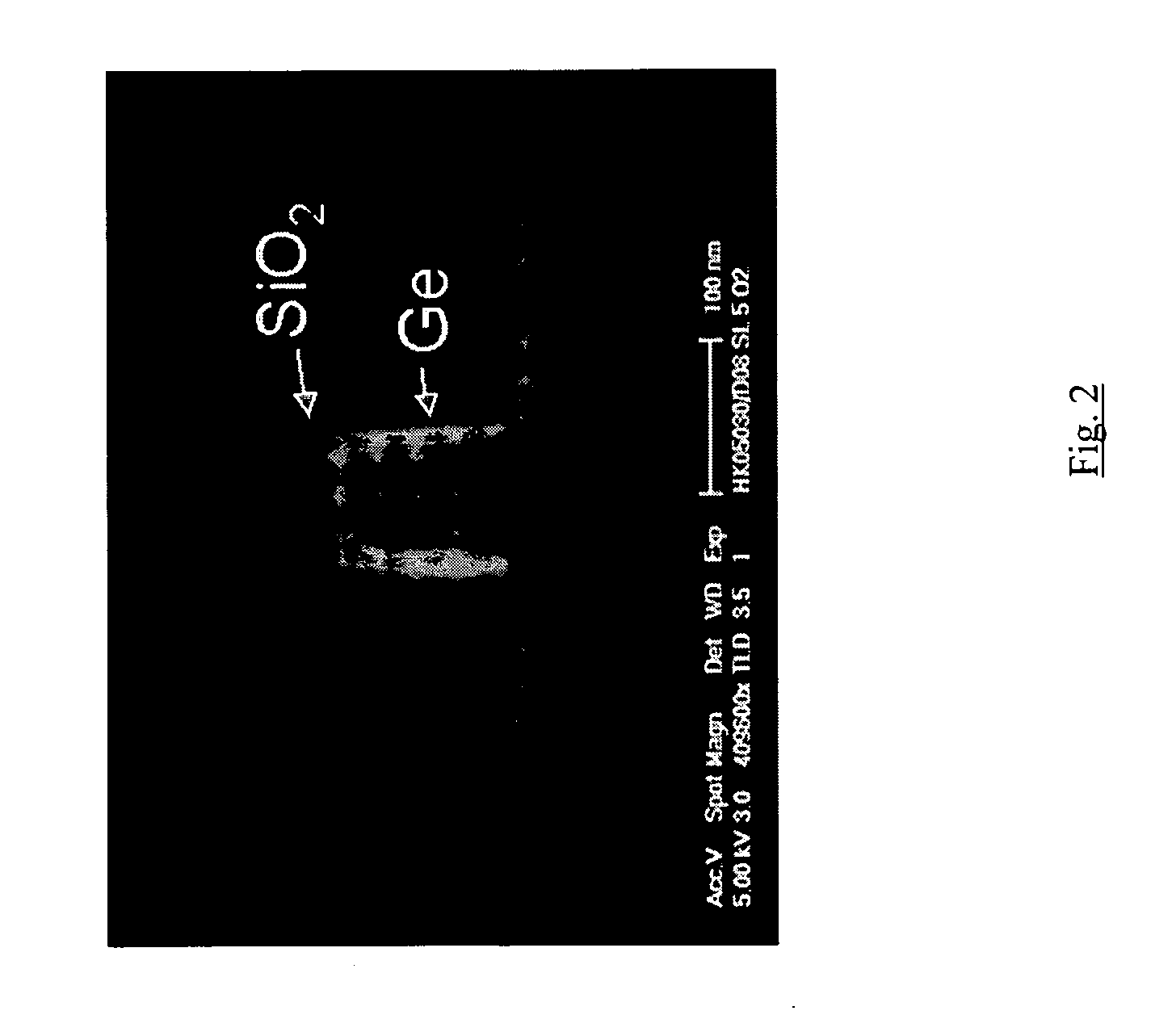
[0103] The BCl3 / N2 plasma was used to pattern pure Ge gates having a high-k dielectric underneath (in the presented case the high-k dielectric is HfO2). The high-k dielectric must be removed selectively to the underlying Si substrate.

[0104] The Ge gate profile just after patterning and before high-k removal as shown in FIG. 2 is straight.

[0105] The conventional way of HfO2 removal is etching in BCl3 plasma. If high-k is removed by such plasma, the Ge gate suffers from profile distortion while addition of 10% N2 to the BCl3 plasma preserves the profile even if the removal time is doubled as shown in FIG. 3.

[0106]FIG. 3A shows the Ge gate profile after high-k removal by a pure BCl3 plasma for 10 seconds and FIG. 3B shows the Ge gate profile after high-k removal by a BCl3 / N2 (10% N2) plasma for 20 seconds. No lateral attack of the Ge profile is seen in FIG. 3B.

[0107] It can be concluded that addition of small amounts of...

example 3

Plasma Parameters Used to Deposit a BxNy Passivation Film

[0108] The plasma parameters used for the deposition of a BxNy passivation film during TaN metal gate patterning as presented in Example 1 using a plasma of a preferred embodiment are as follows: pressure 0.666 Pa (5 mT), plasma power 450 W, flow BCl3 95 sccm (standard centimeter cube per minute), flow N2 5 sccm, and substrate bias 55V.

[0109] The plasma parameters used for the deposition of a BxNy passivation film during high-k removal in a Ge gate stacks as presented in Example 2 are as follows: pressure 0.666 Pa (5 mT), plasma power 450 W, substrate bias 30V, BCl3 90 sccm, N2 10 sccm.


PUM


Abstract

A plasma composition and its use in a method for the dry etching of a stack of at least one material chemically too reactive towards the use of a Cl-based plasma are provided. Small amounts of nitrogen (5% up to 10%) can be added to a BCl3 comprising plasma and used in an anisotropical dry etching method whereby a passivation film is deposited onto the vertical sidewalls of stack etched for protecting the vertical sidewalls from lateral attack such that straight profiles can be obtained.

Description

CROSS-REFERENCE TO RELATED APPLICATIONS [0001] This application claims the benefit under 35 U.S.C. § 119(e) of U.S. provisional application Ser. No. 60 / 731,608, filed Oct. 28, 2005, and U.S. provisional application Ser. No. 60 / 839,897, filed Aug. 23, 2006, the disclosures of which are hereby expressly incorporated by reference in their entirety and are hereby expressly made a portion of this application.FIELD OF THE INVENTION [0002] A method of dry etching of advanced gate stacks is provided which can be used to etch metal gate comprising stacks and pure germanium comprising stacks. An etch plasma composition is also provided for dry etching of metal gate comprising stacks and pure germanium comprising stacks, thereby preserving the vertical profile of the gate stack after patterning. BACKGROUND OF THE INVENTION [0003] As the critical dimensions in CMOS manufacturing shrink for the 90 nm technology node and beyond, conventional (poly) silicon gates are being replaced by metal gates ...

Claims


Application Information

Patent Timeline
IPC IPC(8): H01L21/302H01L21/461
CPCH01L21/2807H01L21/28088H01L21/31122H01L21/32136H01L29/513H01L29/517H01L29/78
Inventor SHAMIRYAN, DENISPARASCHIV, VASILEDEMAND, MARCBOULLART, WERNER
Owner INTERUNIVERSITAIR MICRO ELECTRONICS CENT (IMEC VZW)
Why Eureka
Try Eureka