Method of making thin film transistor liquid crystal display
- Summary
- Abstract
- Description
- Claims
- Application Information
AI Technical Summary
Benefits of technology
Problems solved by technology
Method used
Image
Examples
Embodiment Construction
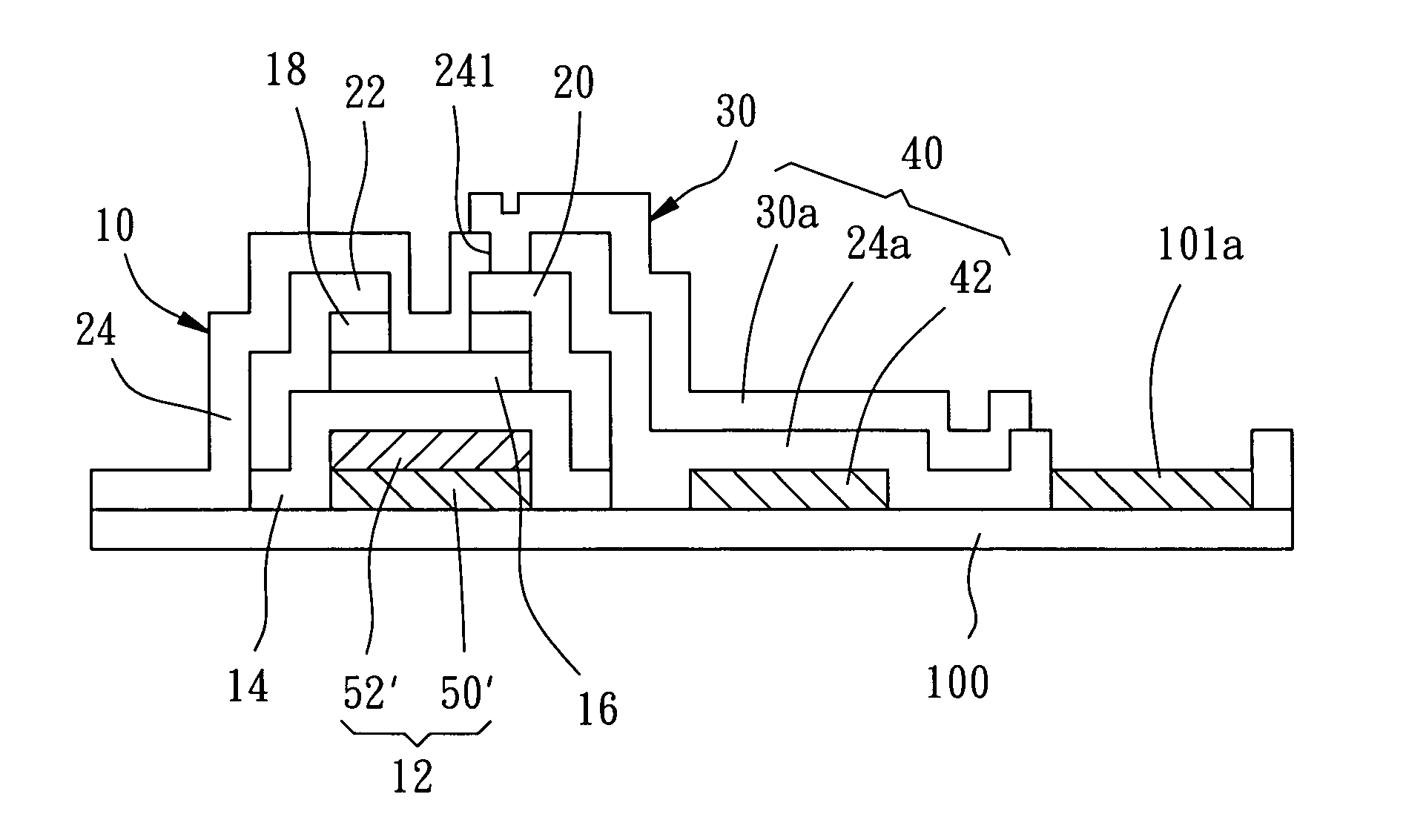
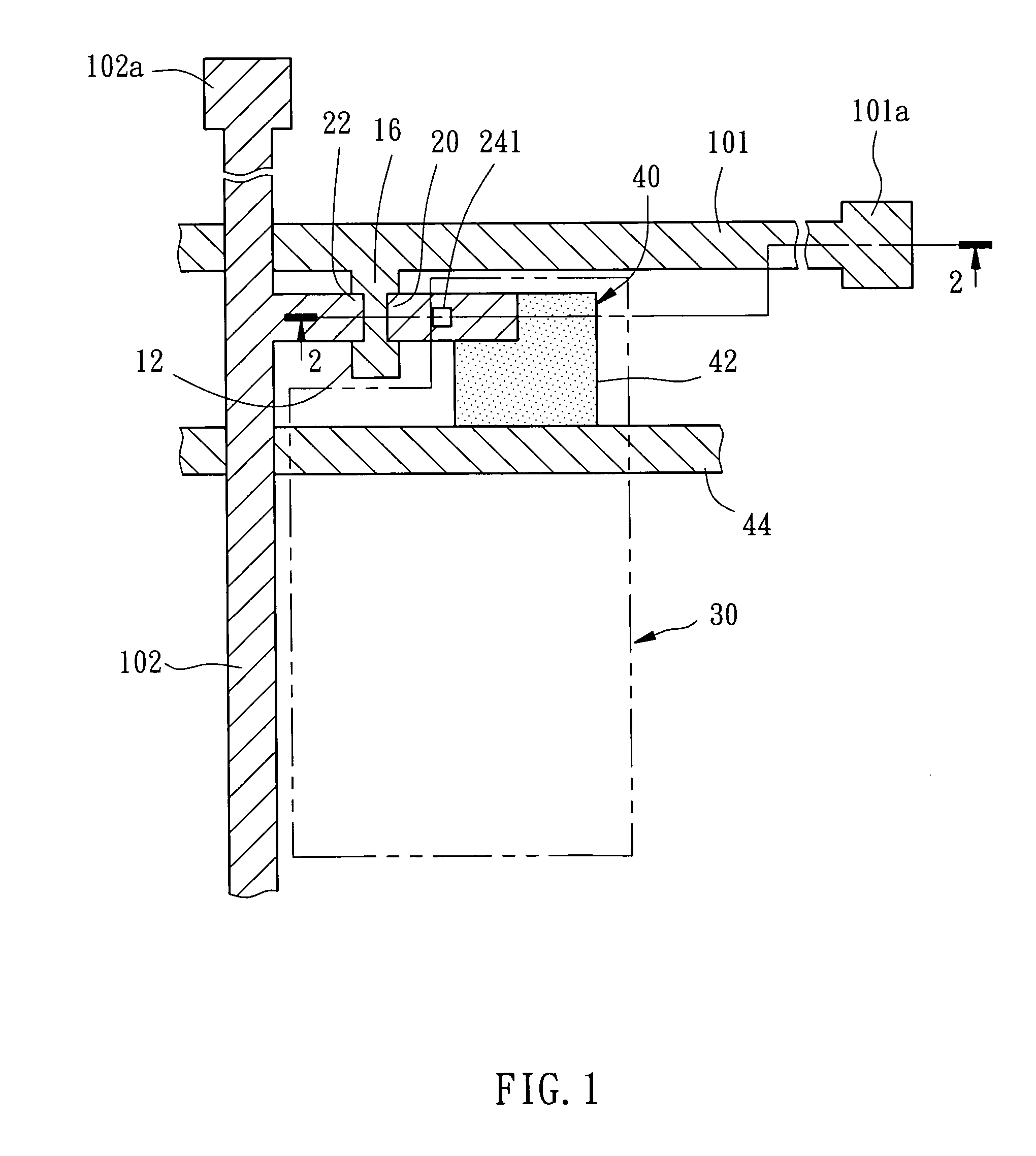
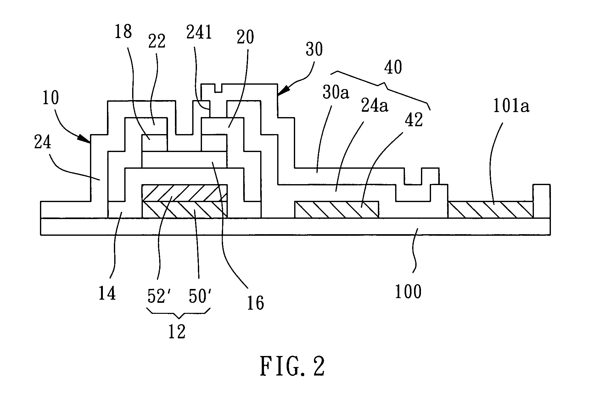
[0023] As shown in FIGS. 1 and 2, a thin film transistor array substrate of the preferred embodiment of the present invention includes a transparent substrate 100 with a plurality of scan lines 101 and data lines 102 thereon. The scan lines 101 and the data lines 102 are perpendicular and cross to each other to form a plurality of subpixels therebetween. The scan lines 101 have a first terminal portion 101a at an end thereof, and the data lines 102 have a second terminal portion 102a at an end thereof. The first terminal portion 101a and the second terminal portion 102a are electrically connected to a driving circuit. Each of the subpixels have an amorphous silicon thin film transistor (a-Si TFT) 10, a pixel electrode 30 and a storage capacitor (Cst) 40. These components are described hereunder:
[0024] The a-Si TFT 10 is an island-like structure with layers (from a bottom to a top) including a gate 12, a gate insulating layer 14, a channel layer 16, an ohmic contact layer 18, a sour...
PUM
 Abstract
Description
Claims
Application Information


