Layout analysis method and apparatus for semiconductor integrated circuit

a technology of integrated circuits and analysis methods, applied in the direction of originals for photomechanical treatment, instruments, program control, etc., can solve the problems of further reduction of power consumption, further increase of operation speeds, and simulation that does not completely conform to actual variations, so as to improve the analysis accuracy of transistor characteristics

Inactive Publication Date: 2007-05-10
SOCIONEXT INC
View PDF6 Cites 5 Cited by
  • Summary
  • Abstract
  • Description
  • Claims
  • Application Information

AI Technical Summary

Benefits of technology

[0010] The present invention provides a layout analysis method and layout analysis apparatus for generating physical parameter distribution enabling accurate recognition of changes in transistor characteristics caused by systematic variations through simulations by improving the analysis accuracy of transistor characteristics.

Problems solved by technology

Thus, designing that provides excessive margins hinder reduction in further reduction in power consumption and further increase in operation speeds.
However, since the parameters for the expressions are stored as a device parameter group associated with devices, the simulation does not completely conform to the actual variations.

Method used


Image

  • Layout analysis method and apparatus for semiconductor integrated circuit
  • Layout analysis method and apparatus for semiconductor integrated circuit
  • Layout analysis method and apparatus for semiconductor integrated circuit

Examples


Embodiment Construction

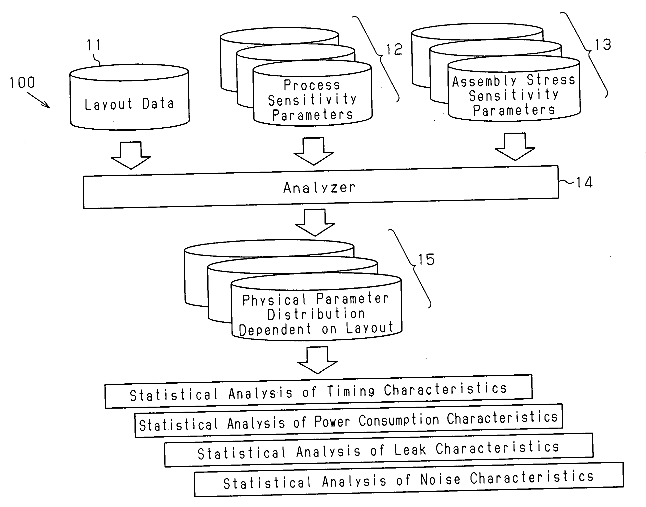
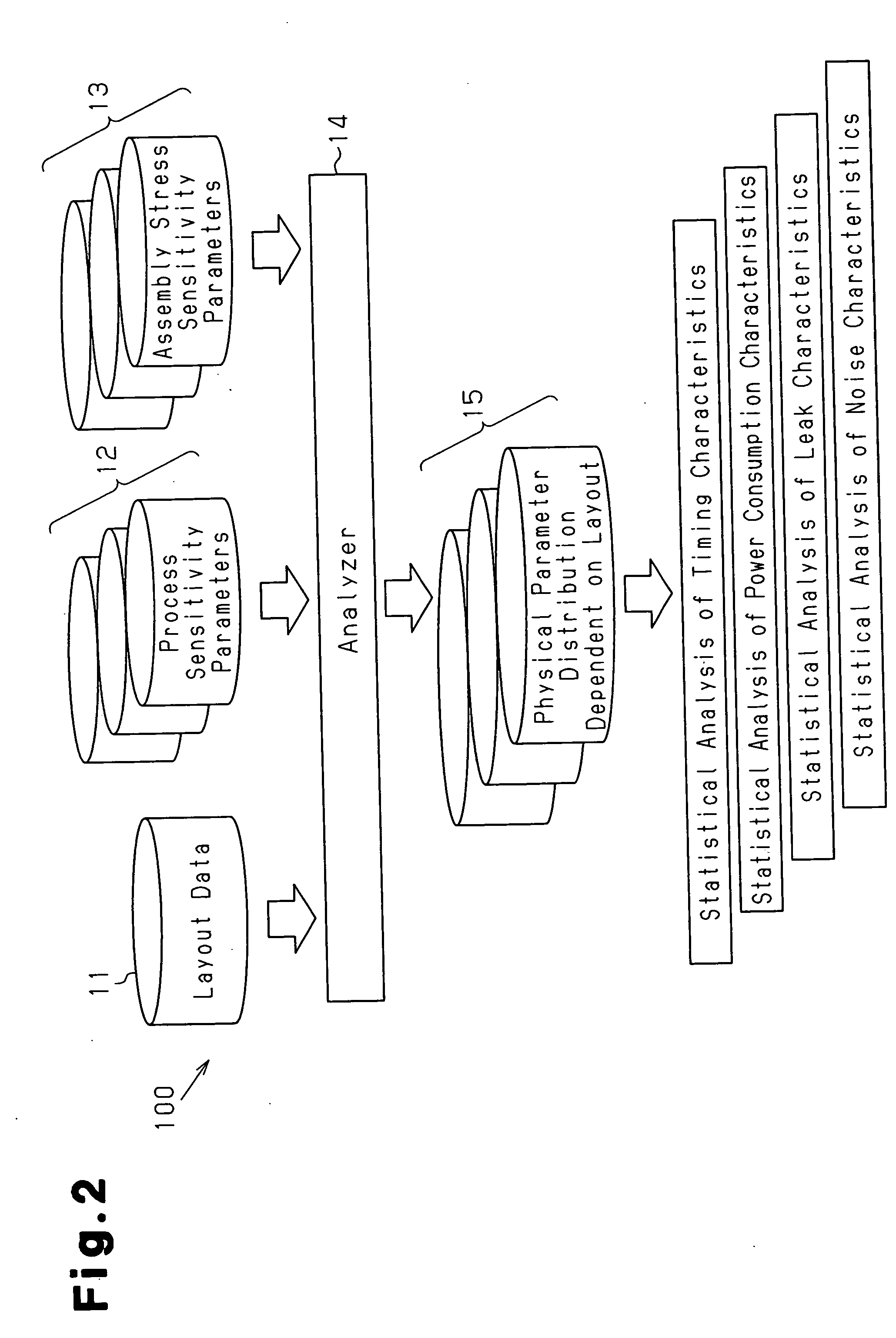
[0029] A layout analysis method and apparatus for a semiconductor integrated circuit according to a preferred embodiment of the present invention will now be discussed. FIG. 2 shows a layout analysis apparatus 100. The layout analysis apparatus 100 includes a first library 11, a second library 12, a third library 13, and an analyzer 14.

[0030] The first library 11 stores layout pattern data, which is generated beforehand. In the preferred embodiment, the first library 11 stores layout patterns of cells or macros laid out for each chip or macro.

[0031] The second library 12 stores various types of process sensitivity parameters. The third library 13 stores various types of assembly stress sensitivity parameters.

[0032] The process sensitivity parameters stored in the second library 12 are tables associated with systematic factors that are dependent on the layout of the semiconductor integrated circuit, such as the pattern shapes of physical devices like transistors, the density (inte...


PUM


Abstract

A method for analyzing a layout for a semiconductor integrated circuit, which includes a plurality of physical devices, to generate physical parameter distribution enabling accurate recognition of changes in transistor characteristics caused by systematic variations. The method includes holding systematic variation tables for physical parameters dependent on the layout of the semiconductor integrated circuit among physical parameters related to characteristics of the semiconductor integrated circuit, analyzing a design layout pattern of the semiconductor integrated circuit and selecting tables corresponding to the plurality of physical devices, and generating a physical parameter distribution based on the selected tables.

Description

CROSS-REFERENCE TO RELATED APPLICATIONS [0001] This application is based upon and claims the benefit of priority from prior Japanese Patent Application No. 2005-323807, filed on Nov. 8, 2005, the entire contents of which are incorporated herein by reference. BACKGROUND OF THE INVENTION [0002] The present invention relates to a layout analysis method and apparatus for analyzing systematic variations in a semiconductor integrated circuit and generating a physical parameter distribution that depends on the layout. [0003] Large-scale integrated circuits (LSIs) have increasingly been miniaturized in recent years. For such miniaturized LSIs, variations in layout patterns and arrangements of circuit elements or variations in manufacturing processes greatly affect circuit performance. Systematic variations (variations for which cause can be identified using design data) cannot be distinguished from random variations (variations for which cause cannot be identified using design data) in pres...

Claims


Application Information

Patent Timeline
Patent Type & Authority Applications(United States)
IPC IPC(8): G06F17/50
CPCG06F17/5081G06F30/398
Inventor INOUE, YOSHIOYONEDA, TAKASHIITO, MASARU
Owner SOCIONEXT INC
Why Eureka
Try Eureka