Supercharge Your Innovation With Domain-Expert AI Agents!

Methods of Manufacturing Light Emitting Devices

a technology of light-emitting devices and manufacturing methods, which is applied in the direction of semiconductor devices, basic electric elements, electrical appliances, etc., can solve the problems of mechanical damage and adhesion problems, the difficulty of achieving the effect of two or more factors in improving the lee, and the difficulty of achieving the effect of reducing manufacturing costs, improving yield, and improving light extraction

Inactive Publication Date: 2007-05-17
ENFOCUS ENG CORP
View PDF8 Cites 127 Cited by
  • Summary
  • Abstract
  • Description
  • Claims
  • Application Information

AI Technical Summary

Benefits of technology

[0005] An aspect of the present invention provides improved light extraction from light emitting devices. It is a further objective of the present invention to replace hard-to-control manufacturing process with more mature processes, thereby, improving yield and reducing manufacturing cost.

Problems solved by technology

Despite these advances, a factor of two or more in improvement of LEE remains to be a severe challenge for manufacturers to reach the ideal goal of unity.
Furthermore, one common disadvantage of these techniques is that they require strenuous mechanical processing, and suffer from mechanical damages and adhesion issues.
These processes are hard-to-control and suffer yield and throughput problems, thus, resulting in high manufacturing cost.
However, to our knowledge, none of these methods are adopted by LED manufacturers since their disclosure in 1998.

Method used


Image

  • Methods of Manufacturing Light Emitting Devices
  • Methods of Manufacturing Light Emitting Devices
  • Methods of Manufacturing Light Emitting Devices

Examples


examples

[0045] Some exemplary manufacturing techniques for some embodiments of the present invention will now be described to enable those skilled in the art to readily adapt the teachings of the present invention into a multiplicity of alternative material combinations and known processing techniques.

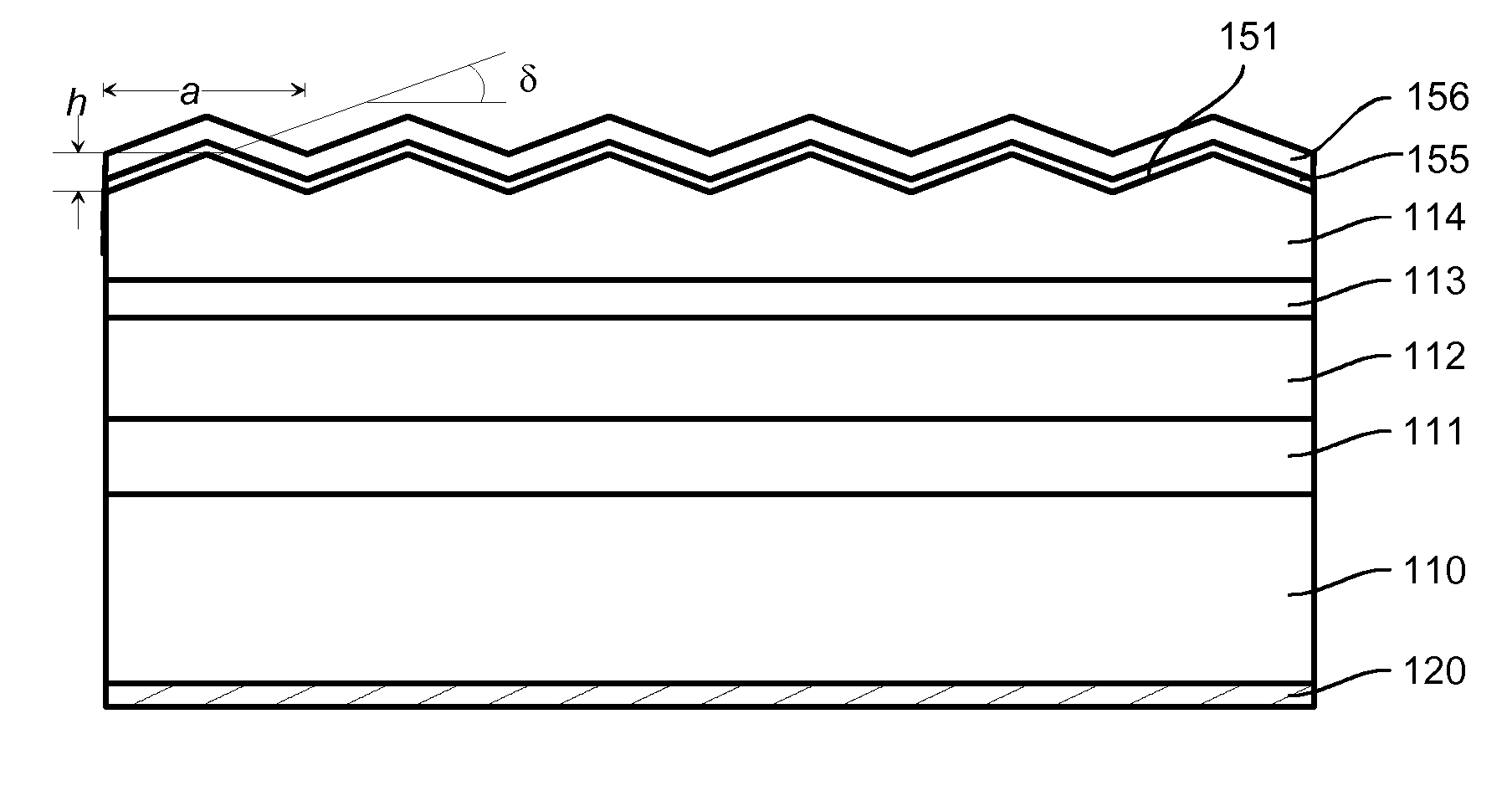
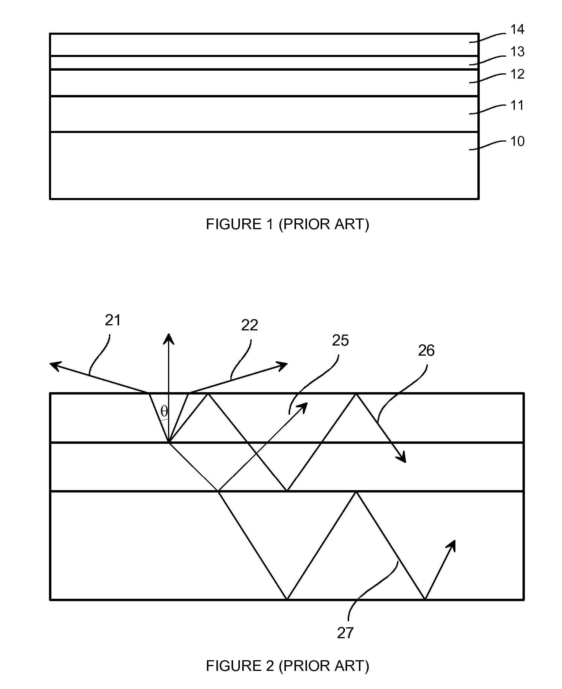
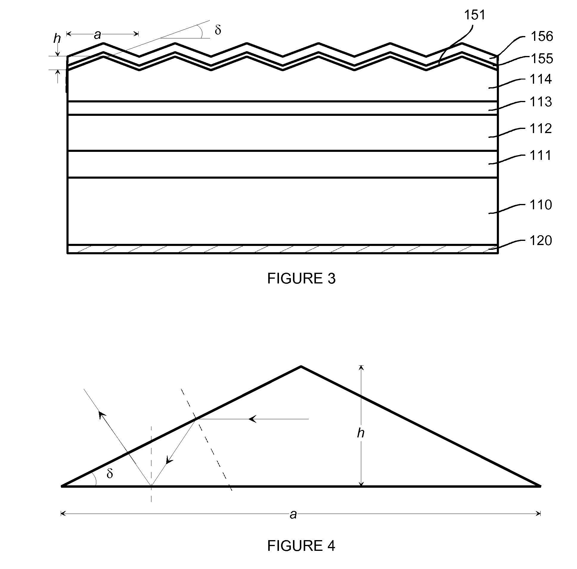
[0046] InAlGaN p-up LED on sapphire, First Embodiment: [0047] 1) Epi growth using Metal Organic Chemical Vapor Phase Deposition (MOCVD): [0048] a) Start with sapphire substrate, 110. [0049] b) Grow nucleation layer, GaN or AlN, or multilayer of InAlGaN / GaN, 10 to 100 nm thick. [0050] c) Grow a thick GaN buffer layer, 111, 0.5 to 5 μm, undoped or lightly doped with Si. [0051] d) Grow n-type GaN, 112, 0.5-5 μm, doped with Si. [0052] e) Grow InGaN / GaN multiple quantum wells (MQW) as the active region, 113, for light emission, 2 to 20 pairs, InGaN quantum wells (QW) are ˜2-4 nm thick, indium composition is controlled by growth temperature and trimethylindium flow rate to achieve targeted emission...


PUM


Abstract

Light emitting devices (LED) and methods of fabricating such, comprising a substrate, a light extraction structure, and an emitting layer sandwiched between a plurality of semiconductor layers of the first and the second type. The said extraction structure is processed into preferred geometric shapes using preferred methods.

Description

FIELD OF INVENTION [0001] The present invention is in the field of light emitting devices such as a light emitting diodes (LEDs) or organic light emitting diodes (OLEDs), and more particularly to the enhanced light escaping or extraction from emitters. BACKGROUND ART [0002] As illustrated in FIG. 1, a solid state light emitting device (LED) typically consists of a light emitting layer, 13, sandwiched between an electron injection layer (n-type) and a hole injection layer (p-type), 12 and 14. The LED stack (12 through 14) is attached to a supporting substrate, 10, either in a n up (14 is n-type), or more commonly, a p up (14 is p-type) configuration. The substrate may either be the natural growth substrate or mounted later using wafer bonding techniques. An intermediate layer, 11, is commonly formed between the LED stack and the substrate, being a buffer layer, multi-layer reflector, or a metal adhesion and / or reflector. The LED stack may face up as in most common LEDs, or may face d...

Claims


Application Information

Patent Timeline
IPC IPC(8): H01L33/00H01L33/22H01L33/46
CPCH01L33/22H01L33/46H01L51/5275H10K50/858
Inventor LU, ZHENGHAO JASON
Owner ENFOCUS ENG CORP
Features
  • R&D
  • Intellectual Property
  • Life Sciences
  • Materials
  • Tech Scout
  • Unparalleled Data Quality
  • Higher Quality Content
  • 60% Fewer Hallucinations
Learn More