Electronic component

a technology of electronic components and components, applied in the field of electronic components, can solve the problems of increasing the possibility of shorting failure, dielectric loss, and increasing the transmission loss of capacitors in the operational frequency range, and achieve the effect of preventing electromigration and accurate capacity values

Active Publication Date: 2007-05-17
TDK CORPARATION
View PDF12 Cites 18 Cited by
  • Summary
  • Abstract
  • Description
  • Claims
  • Application Information

AI Technical Summary

Benefits of technology

[0022] It is an object of the invention to provide an electronic component whose capacitor element has an accurate capacity value and in which electromigration can be prevented.
[0036] The invention makes it possible to provide an electronic component whose capacitor element has an accurate capacity value and in which electromigration can be prevented.

Problems solved by technology

However, the use of a dielectric film made of a material having a great dielectric constant results in an increase in a dielectric loss tangent, which consequently results in an increase in transmission loss of a capacitor in the operational frequency range thereof.
In this case, sufficient insulation may not be provided between the bottom conductor 421 and the top conductor 423 at the edges of the bottom conductor 421, which increase the possibility of a shorting failure.
As a result, a breakdown limit of the withstand voltage of the capacitor element 411 may be lowered, and a problem therefore arises in that the quality of products becomes inconsistent in terms of voltage withstanding capability.
However, an increase in the thickness of the dielectric film 431 necessitates an increase in the electrode area of the capacitor element 411 in order to obtain a great capacity, which results in a problem in that it becomes difficult to make the electronic component compact.
Further, the use of a multi-layer top conductor does not necessarily result in an increase in the capacity of a capacitor.
Further, bottom conductors of capacitors according to the related are uneven in the shape of edges thereof.
When such edges are used as part of electrodes of the capacitors, there will be significant variations in the electrode area, and the capacity value cannot be accurately controlled.
However, since a reduction in the width of the lead-out conductor results in an increase in the parasitic inductance, there will be problems including degradation of high-frequency characteristics of the electronic component and an increase in transmission loss.
However, in the capacitor element disclosed in Patent Document 1, since the top electrode is formed also in the same layer as the bottom electrode so as to face the bottom electrode with the insulator layer interposed between them, a parasitic capacity is generated between the electrodes.
Since the insulator layer is formed to protrude above the substrate surface, it is difficult to provide the dielectric layer in a multi-layer structure.
Further, the configuration makes it difficult to provide a composite component having a plurality of circuit elements in a small size because circuit elements such as an inductor element cannot be formed close to the capacitor element.
The use of an organic material as the material of an insulation film results in the problem of occurrence of electromigration.
Electromigration can consequently cause breakage or shorting of a metal wiring which results in a failure of an electronic component.
However, a separate step is required to form a conductor for preventing electromigration, and which results in the problem of an increase in the manufacturing cost.

Method used


Image

  • Electronic component
  • Electronic component
  • Electronic component

Examples


first embodiment

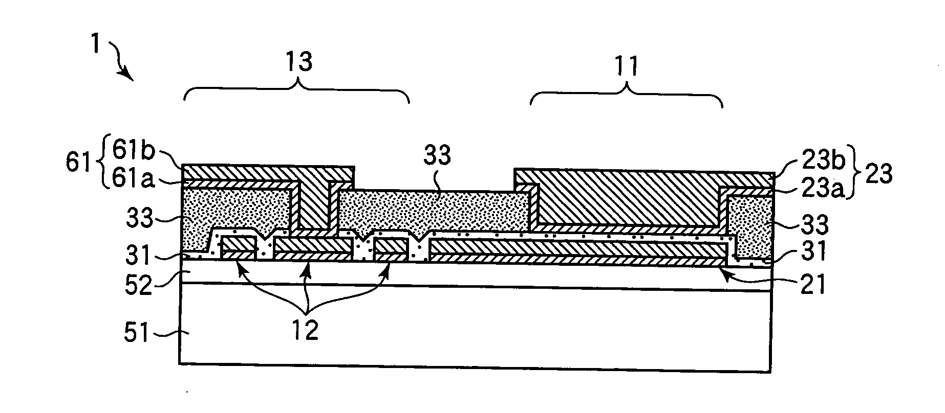
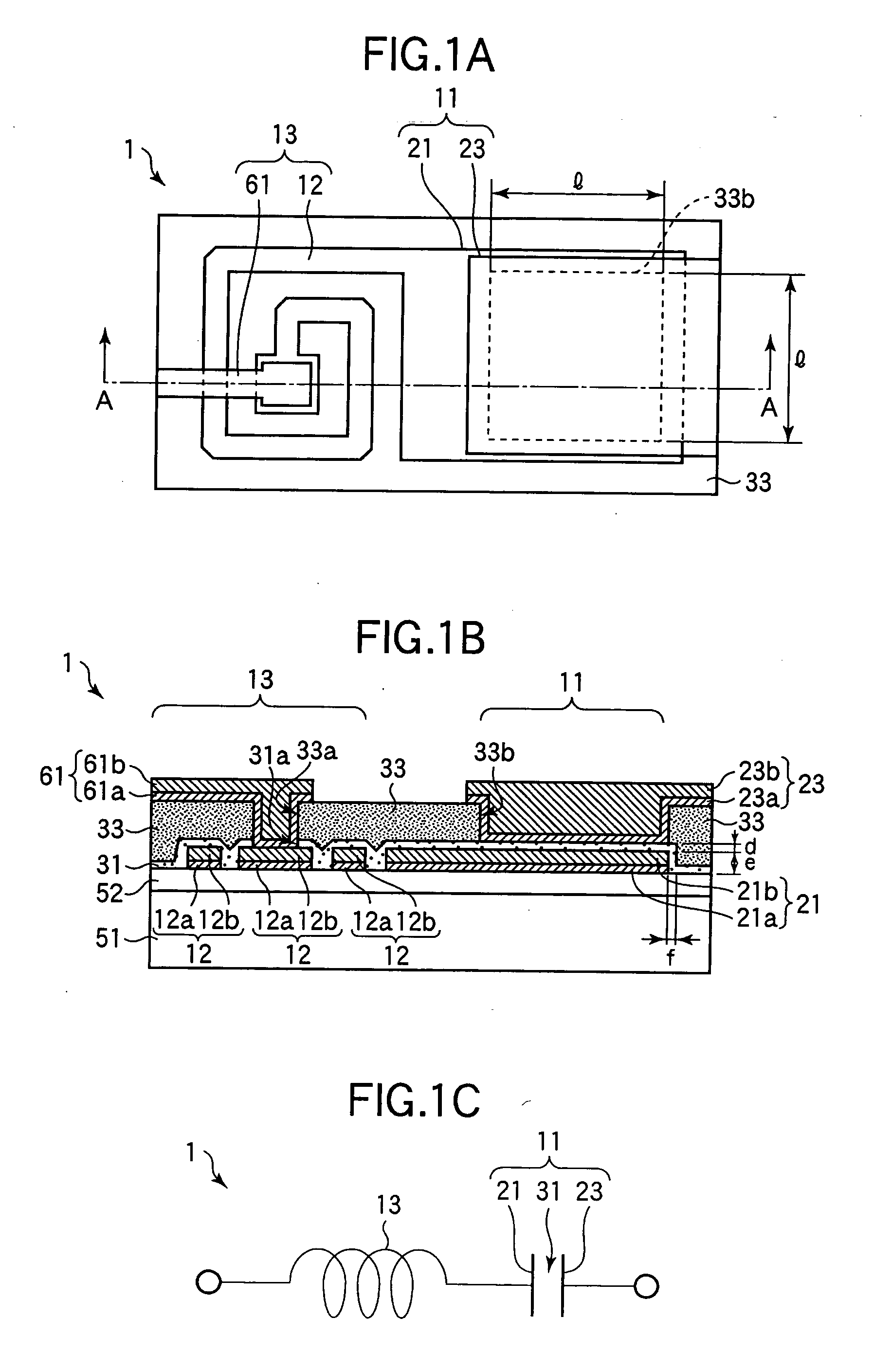
[0056] An electronic component according to a first embodiment of the invention will now be described with reference to FIGS. 1A to 10B. First, an electronic component 1 of the present embodiment will be described with reference to FIGS. 1A to 1C. FIG. 1A is a plan view of the electronic component 1, and FIG. 1B is a sectional view taken along the line A-A in FIG. 1A. FIG. 1C is an equivalent circuit diagram of the electronic component 1. In FIG. 1A, hidden lines are indicated by broken lines.

[0057] As shown in FIGS. 1A and 1B, the electronic component 1 includes a capacitor element (capacity) 11 and an inductor element (circuit element) 13 which are formed using thin-film forming techniques, and the component has a general outline in the form of a rectangular parallelepiped. Referring to FIG. 1A, the length of the longer sides of the electronic component 1 extending in the horizontal direction and the length of the shorter sides of the same extending in the vertical direction in t...

modification 1

(Modification 1)

[0113] An electronic component 2 according to Modification 1 of the present embodiment will be first described with reference to FIGS. 7A and 7B. FIG. 7A is a plan view of the electronic component 2 of the present modification showing only conductors and a dielectric film 31 constituting a capacitor element 11. FIG. 7B shows an equivalent circuit of the electronic component 2. As shown in FIG. 7A, in the electronic component 2, a part of a coil conductor 12 having a spiral shape which is located at an outer end of the conductor serves as a bottom conductor 21 of a capacitor element 11. As shown in FIG. 7B, the capacitor element 11 and an inductor element 13 are connected in series to form a series resonance circuit. Each of a lead-out conductor 61 and a top conductor 23 serves as a terminal for energization.

modification 2

(Modification 2)

[0114] An electronic component 3 according to Modification 2 of the present embodiment will be described with reference to FIGS. 8A and 8B. FIG. 8A is a plan view of the electronic component 3 of the present modification showing only conductors and a dielectric film 31 constituting a capacitor element 11. FIG. 8B is an equivalent circuit diagram of the electronic component 3. As shown in FIG. 8A, an inductor element 13 includes a coil conductor 12 having a spiral shape and a rectangular lead-out conductor 61 connected to an inner end of the coil conductor 12 and extending in the horizontal direction of the figure. The capacitor element 11 includes a rectangular bottom conductor 21 formed integrally with the coil conductor 12, connected to an outer end of the coil conductor 12, and extending in the horizontal direction of the figure and an L-shaped top conductor 23 formed integrally with the lead-out conductor 61 and provided to face the bottom conductor 21. As shown ...


PUM


Abstract

The invention relates to an electronic component including a capacitor and provides an electronic component in which electromigration can be prevented and whose capacitor element has an accurate capacity value. The electronic component includes a bottom conductor formed on a substrate, a dielectric film formed to cover the bottom conductor, an organic insulation film formed on the dielectric film, and a top conductor formed in an opening provided in the organic insulation film over the bottom conductor, the top conductor forming a capacitor element in combination with the bottom conductor and the dielectric film.

Description

BACKGROUND OF THE INVENTION [0001] 1. Field of the Invention [0002] The present invention relates to an electronic component having a capacitor element. [0003] 2. Description of the Related Art Various types of surface-mount electronic components are mounted on a circuit inside an electronic apparatus such as a personal computer or portable telephone. Known surface-mount electronic components include thin-film type electronic components formed using thin film forming techniques. [0004] Thin-film electronic components include thin-film capacitors, thin-film inductors, thin-film LC composite components, and thin-film multi-layer components. Composite components having a capacitor include low-pass filters (LPFs), high-pass filters (HPFs), band-pass filters (BPFs), and trap filters which eliminate signals in a predetermined frequency range. Further, those components may be combined to provide electronic components such as diplexers, duplexers, antenna switch modules, and RF modules. [00...

Claims


Application Information

Patent Timeline
Patent Type & Authority Applications(United States)
IPC IPC(8): H01G4/06
CPCH01G4/228H01G4/33H01G4/40H01L23/5223H01L27/016H01L28/60H01L2924/0002H01L2924/00
Inventor KUWAJIMA, HAJIMEFURUYA, AKIRAMIYAZAKI, MASAHIROSHIBATA, MAKOTO
Owner TDK CORPARATION
Why Eureka
Try Eureka