Thin film transistor array panel and method of manufacturing the same

a technology of thin film transistors and array panels, which is applied in the direction of basic electric elements, electrical equipment, semiconductor devices, etc., can solve the problems of poor durability and chemical resistance of low resistivity, and achieve the effect of reducing contamination

Inactive Publication Date: 2007-05-17
SAMSUNG ELECTRONICS CO LTD
View PDF2 Cites 10 Cited by
  • Summary
  • Abstract
  • Description
  • Claims
  • Application Information

AI Technical Summary

Benefits of technology

[0011] The present invention has been made in an effort to provide a thin film transistor array panel and a manufacturing method there

Problems solved by technology

However, a material having low resistivity is generally poor in durability and chemical resistance a

Method used


Image

  • Thin film transistor array panel and method of manufacturing the same
  • Thin film transistor array panel and method of manufacturing the same
  • Thin film transistor array panel and method of manufacturing the same

Examples


Embodiment Construction

[0024] Hereinafter, embodiments of the present invention will be described in detail with reference to the attached drawings such that the present invention can be put into practice by those skilled in the art. As those skilled in the art will realize, the described embodiments may be modified in various different ways, all without departing from the spirit or scope of the present invention.

[0025] In the drawings, the thickness of layers, films, panels, regions, etc., may be exaggerated for clarity. Like reference numerals designate like elements throughout the specification. When it is said that any part, such as a layer, film, area, or plate is positioned “on” another part, it means the part is directly on the other part or above the other part with at least one intermediate part. In contrast, when an element is referred to as being “directly on” another element, there are no intervening elements present.

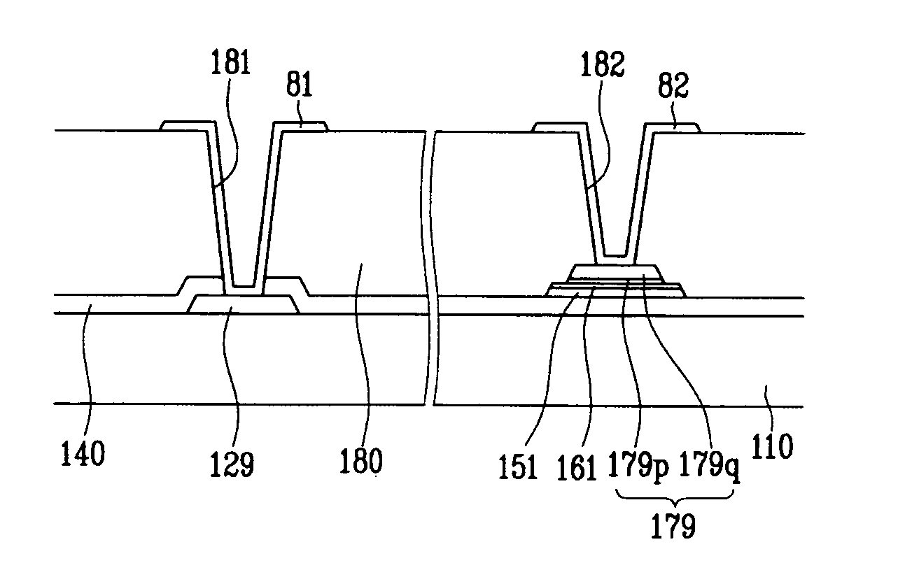
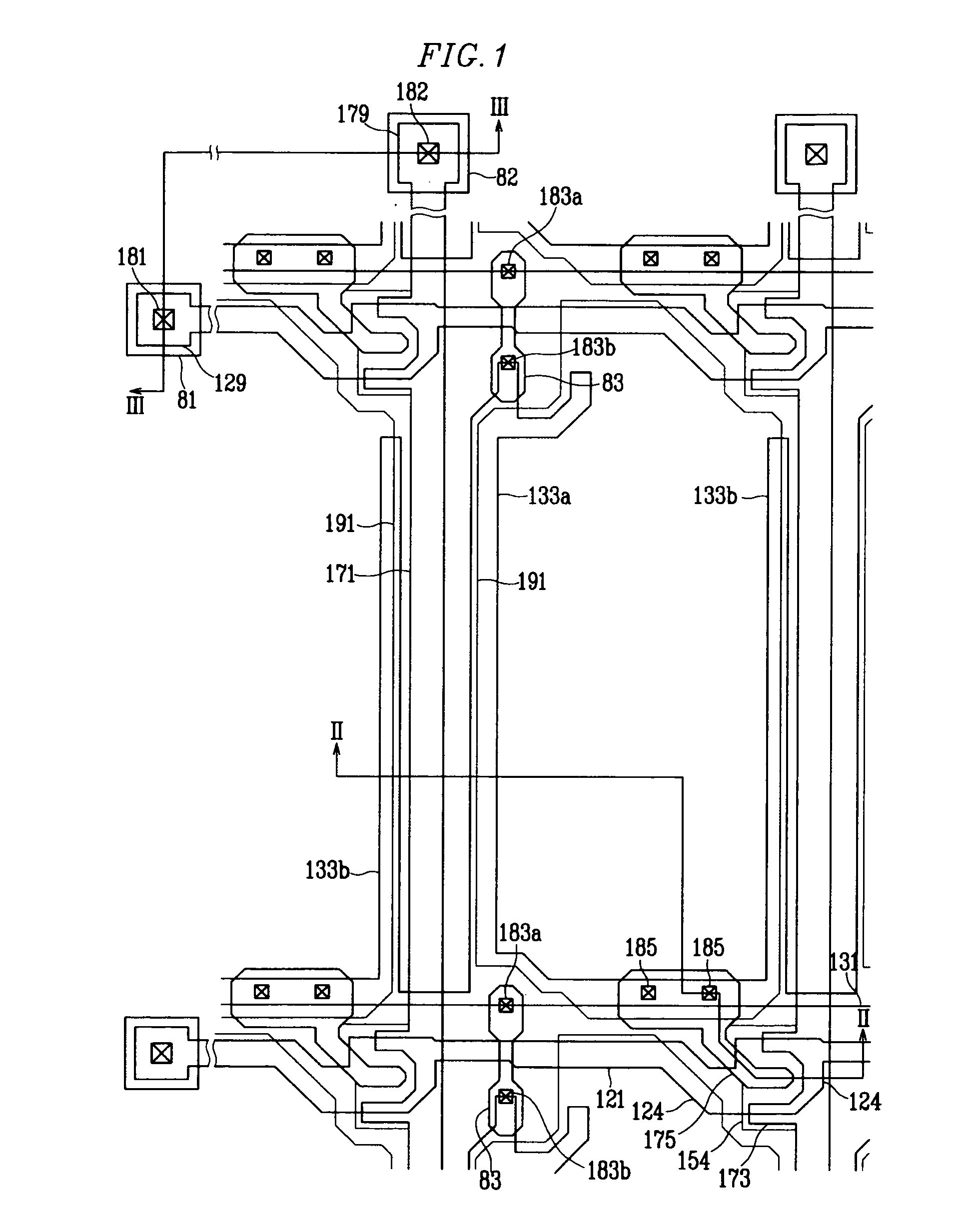
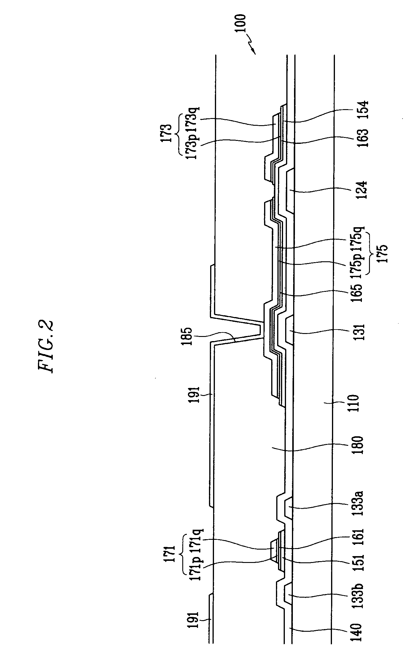
[0026] First, a thin film transistor array panel according to an embodiment...


PUM


Abstract

In one embodiment, a thin film transistor array display panel and method of manufacturing the same are provided. A method includes forming a gate line on a substrate; forming a gate insulating layer, a semiconductor layer, and an ohmic contact layer on the gate line; forming a data layer on the ohmic contact layer; forming a photosensitive pattern on the data layer; etching the data layer to form a data line including a source electrode and a drain electrode that is opposite to the source electrode; reflowing the photosensitive pattern to cover side surfaces of the source electrode and the drain electrode; and etching the ohmic contact layer using the reflowed photosensitive pattern as a mask.

Description

CROSS-REFERENCE TO RELATED APPLICATION [0001] This application claims priority to and the benefit of Korean Patent Application Nos. 10-2005-0110092 and 10-2005-0123526 that were respectively filed in the Korean Intellectual Property Office on Nov. 17, 2005, and Dec. 14, 2006, the entire contents of which are incorporated herein by reference. BACKGROUND [0002] (a) Field of the Invention [0003] The present invention relates to a thin film transistor array panel and a manufacturing method thereof. [0004] (b) Description of the Related Art [0005] In general, a flat panel display such as a liquid crystal display (LCD), an organic light emitting diode (OLED) display, and an electrophoretic display includes a plurality of pairs of field generating electrodes and an electro-optical active layer that is interposed therebetween. The LCD includes a liquid crystal layer as an electro-optical active layer, and the OLED display includes an organic emission layer as an electro-optical active layer...

Claims


Application Information

Patent Timeline
IPC IPC(8): H01L21/84
CPCH01L21/0273H01L21/32139H01L27/1288H01L27/124H01L27/12
Inventor OH, MIN-SEOKPARK, JEONG-MINKIM, SANG-GABCHIN, HONG-KEEJEONG, CHANG-OHPARK, HONG-SICKKIM, SHI-YUL
Owner SAMSUNG ELECTRONICS CO LTD
Why Eureka
Try Eureka