Semiconductor device

a technology of semiconductor devices and semiconductors, applied in semiconductor devices, semiconductor/solid-state device details, electrical apparatus, etc., can solve the problems of noise addition to external input signals, insufficient reduction of mutual inductance, etc., and achieve the effect of parallel input/output operation

Inactive Publication Date: 2007-05-31
RENESAS ELECTRONICS CORP
View PDF2 Cites 66 Cited by
  • Summary
  • Abstract
  • Description
  • Claims
  • Application Information

AI Technical Summary

Benefits of technology

[0011] It is desirable to reduce or suppress induction of a noise from the external output signal system to the external input signal system, in which parallel input / output operation is enabled. In a word, it is desirable to reduce mutual inductance from the external output signal system to the external input signal system, in which parallel input / output operation is enabled.

Problems solved by technology

When current change occurs in a signal transfer system, noise voltage in proportion to self-inductance is produced, in addition, when current change occurs in an adjacent, and different signal transfer system, noise voltage is also produced in proportion to mutual inductance.
However, it is not enough to sufficiently reduce mutual inductance.
First, when the semiconductor integrated circuit having the WPP structure is mounted on the BGA package substrate, a wiring layer as a top layer of the BGA package substrate is directly opposed to leader wirings connecting between the solder bumps and the pad electrodes, and a shield layer is not provided between them.
When a wiring of an external output signal system and wiring of an external input signal system exist as wirings opposed in such a way, a noise are added to an external input signal.

Method used


Image

  • Semiconductor device
  • Semiconductor device
  • Semiconductor device

Examples


Embodiment Construction

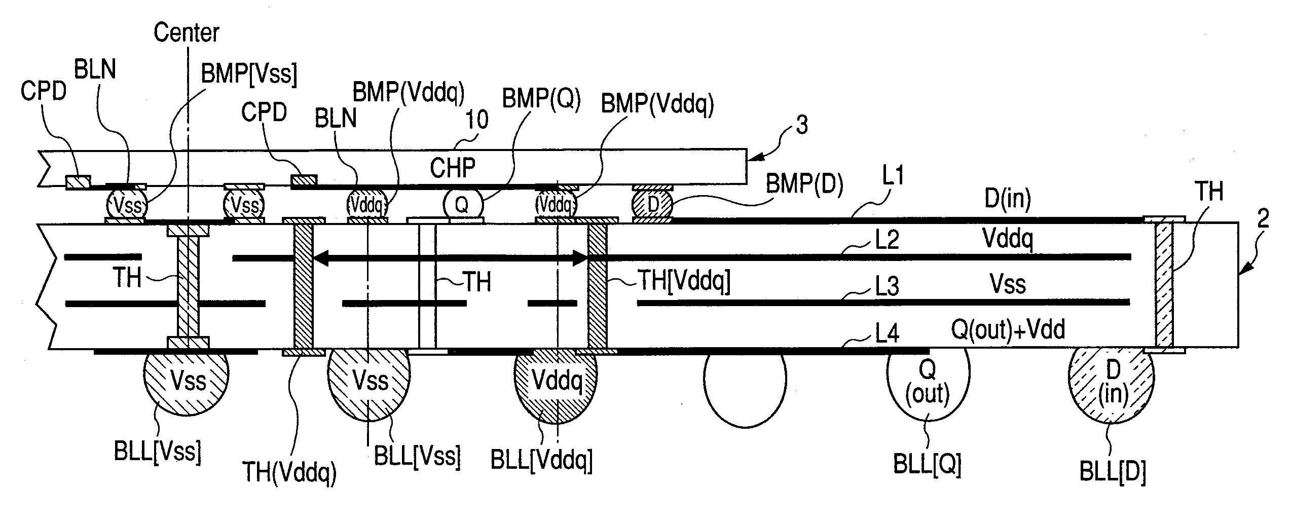
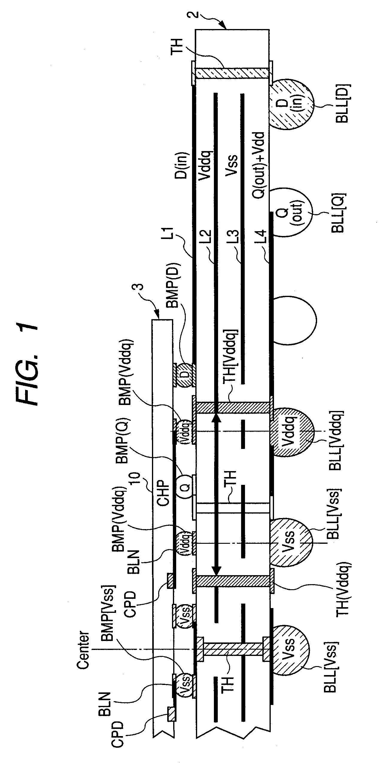
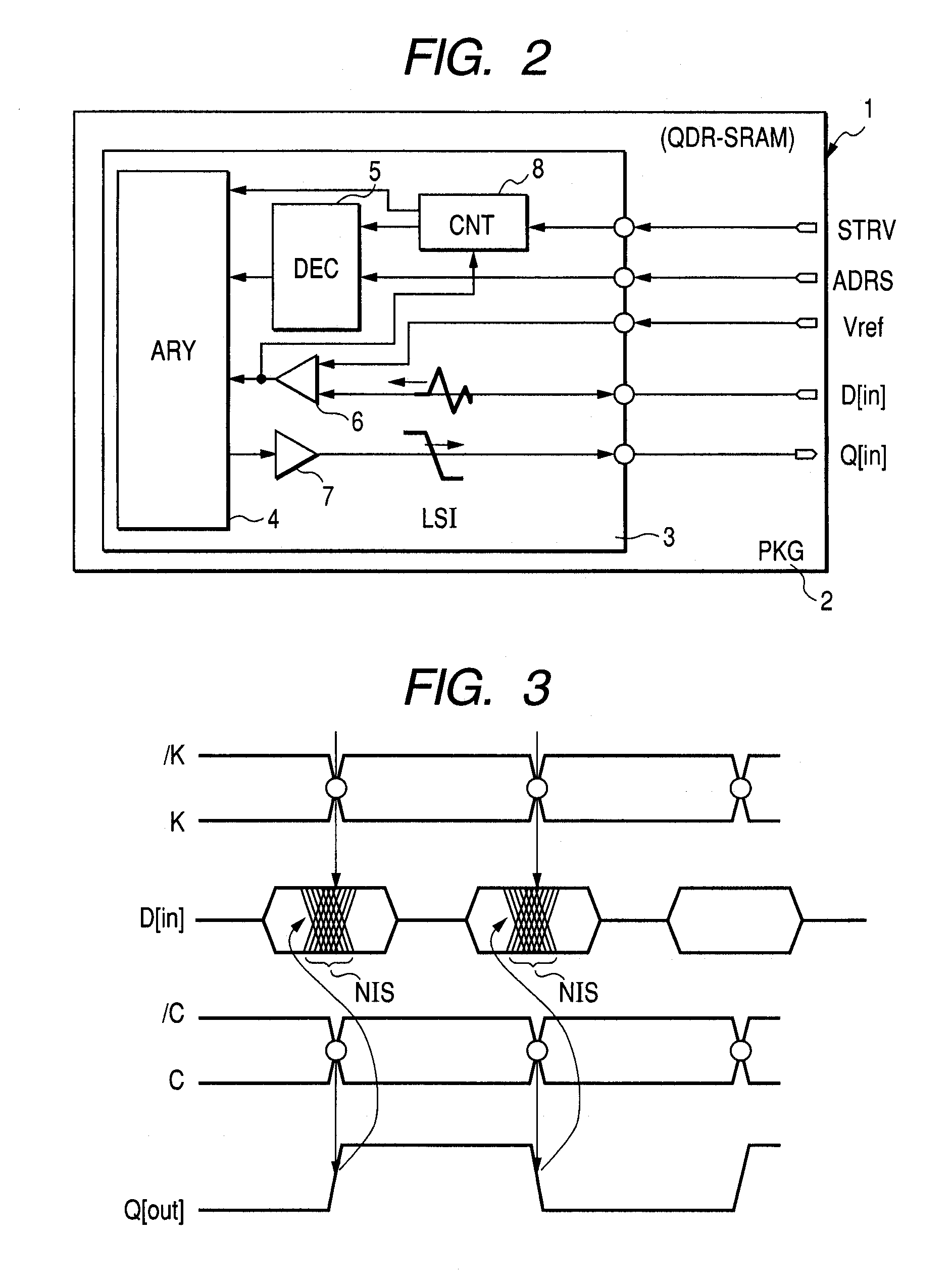
[0070]FIG. 2 shows a block diagram of a quad-static random access memory (QDR-SRAM) as an example of a semiconductor device according to an embodiment of the invention. QDR-SRAM 1 is configured by mounting a semiconductor integrated circuit (LSI) 3 having a WPP structure on a package substrate (PKG) 2 in a full grid, ball grid array (BGA) configuration. In the semiconductor integrated circuit 3, external input and external output of data are enabled in parallel, input and output are synchronized with a specific clock signal respectively, and each operation can be synchronized with a falling edge and a rising edge of a clock signal. Typically, D[in] indicates external input data, Q[out] indicates external output data, Vre indicates reference potential, ADRS indicates an address signal, and STRV indicates an external access control signal. A memory array (ARY) 4 has a plurality of memory banks each of which can independently perform memory operation, and selection of a memory cell is ...


PUM


Abstract

Mutual inductance from an external output signal system to an external input signal system, in which parallel input / output operation is enabled, is reduced. A semiconductor integrated circuit has a plurality of external connection terminals facing a package substrate, and has an external input terminal and an external output terminal, in which parallel input / output operation is enabled, as part of the external connection terminals. The package substrate has a plurality of wiring layers for electrically connecting between the external connection terminals and module terminals corresponding to each other. A first wiring layer facing the semiconductor integrated circuit has a major wiring for connecting between the external input terminal and a module terminal corresponding to each other, and a second wiring layer in which the module terminals are formed has a major wiring for connecting between an external output terminal and a module terminal corresponding to each other. A major signal wiring of an external output system connected to the external output terminal, which may be a noise source, is made to be in a wiring layer distant from the semiconductor integrated circuit.

Description

CROSS-REFERENCE TO RELATED APPLICATIONS [0001] The disclosure of Japanese Patent Application No. 2005-342479 filed on Nov. 28, 2005 including the specification, drawings and abstract is incorporated herein by reference in its entirety. BACKGROUND OF THE INVENTION [0002] 1. Field of the Invention [0003] The present invention relates to a semiconductor device that enables parallel operation of external output and external input, and particularly relates to a technique for reducing a noise caused by an undesired inductance component parasitizing a package substrate mounted with a semiconductor integrated circuit. For example, the invention relates to a technique effective for use in a quad static random access memory (quad SRAM) in which external data output operation timing can be varied with respect to input operation of external multi-bit data. [0004] 2. Description of Related Art [0005] When current change occurs in a signal transfer system, noise voltage in proportion to self-indu...

Claims


Application Information

Patent Timeline
Patent Type & Authority Applications(United States)
IPC IPC(8): H01L23/52
CPCH01L23/49838H01L23/50H01L23/528H01L2924/01046H01L2924/01079H01L2924/15311H01L2924/3011H01L2924/3025H01L2224/16225H01L2924/01019H01L2224/05568H01L2224/05573H01L2924/00014H01L2224/05599H01L23/12
Inventor YOSHIKAWA, YASUHIROSUWA, MOTOOTOYOSHIMA, HIROSHI
Owner RENESAS ELECTRONICS CORP
Why Eureka
Try Eureka