Dual emission display

a dual-emission display and display technology, applied in the direction of discharge tube luminescnet screens, discharge tube/lamp details, electric discharge lamps, etc., can solve the problems of easy damage to elements mounted on the substrate, complicated and time-consuming manufacturing of conventional dual-emission displays b>10/b>, and achieve the effect of preventing particles and simplifying the manufacturing process

Inactive Publication Date: 2007-06-07
AU OPTRONICS CORP
View PDF11 Cites 18 Cited by
  • Summary
  • Abstract
  • Description
  • Claims
  • Application Information

AI Technical Summary

Benefits of technology

[0011] The object of the present invention is to provide a thinner dual emission display which is adapted to simpler fabricating process and capable of preventing particles from damaging the light emitter on the substrate.

Problems solved by technology

Therefore, it becomes larger, thicker, and heavier, so as not to meet the requirement of weight, thickness and size.
The disadvantages is that, when the package lid is pressed to bend or to press the particles generated from the fabricating process, the elements mounted on the substrate is damaged easily by the bended package lid or the pressed particles.
Therefore, the manufacture of the conventional dual emission display 10 is complicated and time-consuming.
Another drawback is that the two display panels 11 and 12 need to be driven independently.
Thus, the cost is increased because no components such as chips or flexible printed circuits (FPCs) are saved.
The typical dual emission display is thicker and is fabricated by more complicated process due to using more components such as package lids and substrates.
The elements mounts on the substrate is damaged easily by the particles generating from the fabricating process.

Method used


Image

  • Dual emission display
  • Dual emission display
  • Dual emission display

Examples


first embodiment

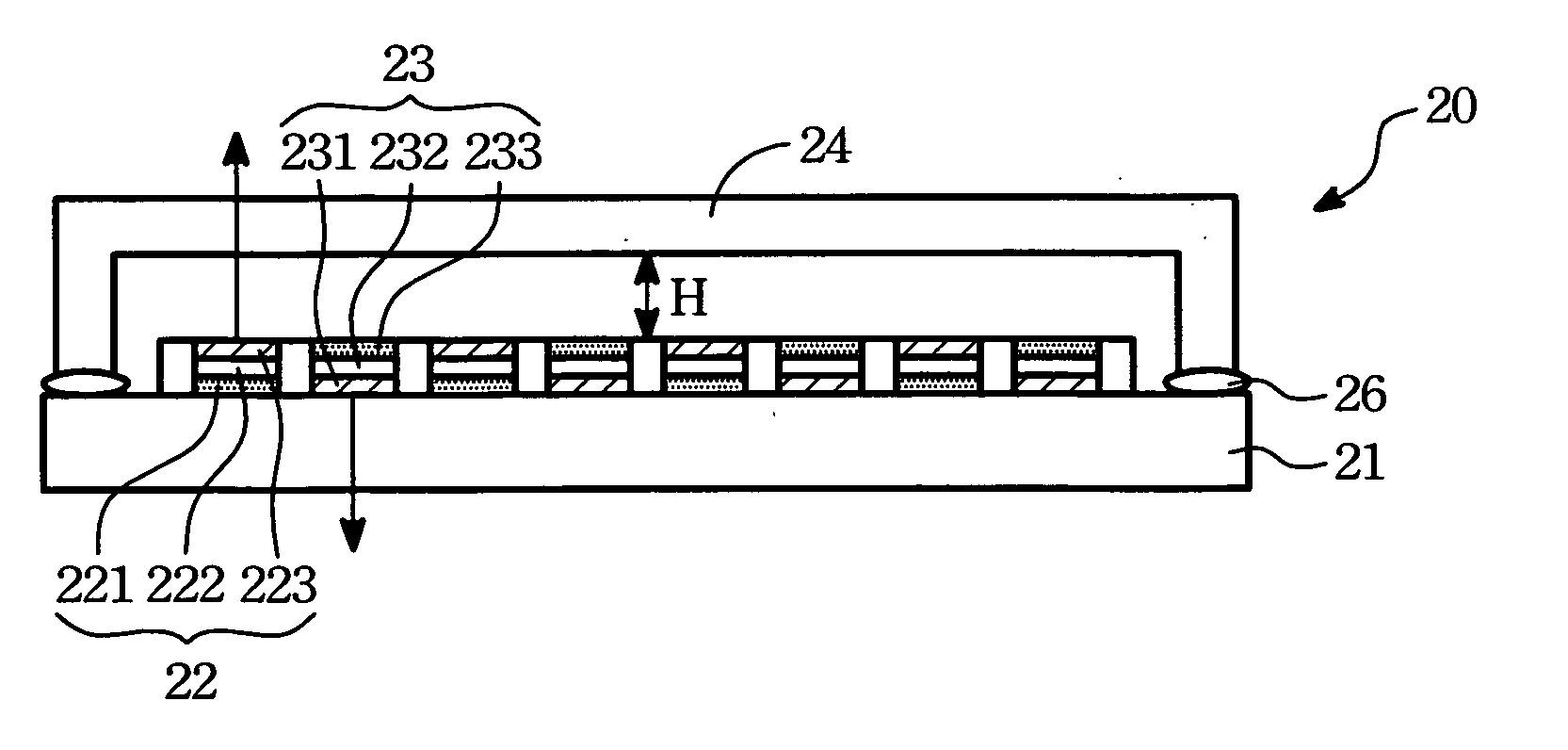
[0021] FIG.2 is the present invention. A dual emission display 20 includes a substrate 21, two sort of light emitters 22 and 23 having different light-emitting directions, and a cap 24. In following description, the substrate 21 and the cap 24 can be made of organic or inorganic materials.

[0022] As shown, the light emitters 22 and 23 are next to each other, and disposed on the same substrate 21. The substrate 21 can be made of glass or plastic. In this embodiment, the dual emission display 20 is capable of displaying images in upper and lower sides since the light emitter 22 emits upward and the light emitter 23 emits downward. The cap 24 is disposed on the light emitters 22 and 23 to prevent external forces from damaging. And also, the cap 24 should be made of the hard materials with light transmissivity of equal to or more than 30 percent, such as glass, hard plastic etc. An adhesive 26 is used to adhere the cap 24 to the substrate 21. A point worth emphasizing is that, there is a...

second embodiment

[0031] FIG.4 is the present invention. A supporting layer is formed in the non-upward emitting area of the dual emission display, in order to isolate the substrate from the glass cap. Thus, the supporting layer prevents the cap from damaging the elements mounted on the substrate. In the dual emission display 30, a spacing layer 31 is sandwiched between the upward emitter 22 and the downward emitter 23. A supporting layer 32 is formed on the spacing layer 31 to prevent the cap 24 from caving downward due to external forces. In order to maintain the efficient distance, the supporting layer 32 should have at least 1 to 100 μm height. However, the materials of the supporting layer 32 are not limited to organic or inorganic materials.

[0032] As above mentioned, the cap 24 has a body with concave-up inner surface. The adhesive 26 is provided to package the substrate 21 to the low edge of the sidewall of the cap 24. In addition, the cap 24 may be replaced with a flat board, shown in FIG.5. ...


PUM


Abstract

A dual emission display includes a substrate, a first light emitter, a second light emitter and a cap. The two light emitters are disposed on the substrate. The first light emitter has a first light-emitting direction. The second light emitter is adjacent to the first light emitter, and has a second light-emitting direction. The cap is located on the first emitter and the second emitter, and is separated from one of the first emitter and the second emitter by a distance ranging from about 1 μm to 100 μm.

Description

[0001] This application claims the benefit of Taiwan Patent Application Serial No. 094142592, filed Dec. 2, 2005, the subject matter of which is incorporated herein by reference. BACKGROUND OF THE INVENTION [0002] (1) Field of the Invention [0003] The present invention relates to dual emission display, and more particularly, to a dual organic electroluminescent display capable of protecting its light emitters from damaging by external forces. [0004] (2) Description of the Prior Art [0005] As the electric products are getting more and more various, they emphasize the structure of two display screens. For example, a mobile phone having a dual emission display can display a main function menu at one side, and display time at the other side. Typically, the dual emission display includes two adhered single-side panels, such as a liquid crystal panel adhered to an organic electro-luminescent panel, two adhered liquid crystal panels, or two adhered organic electro-luminescent panels. [0006...

Claims


Application Information

Patent Timeline
Patent Type & Authority Applications(United States)
IPC IPC(8): H05B33/04H01L51/52
CPCH01L27/3267H01L27/3281H01L51/524H01L51/525H10K59/128H10K59/17H10K50/8428H10K50/841
Inventor CHIU, CHUN-YIHU, MIN-CHIEH
Owner AU OPTRONICS CORP
Why Eureka
Try Eureka