

Power saving method in an integrated circuit programming and control circuit
a power saving and control circuit technology, applied in the field of programming and control of integrated circuits, can solve the problems of unwarranted complexity of the core product, failure to meet the needs of increasingly complex ics, and simple implementation of binary input control logic,
- Summary
- Abstract
- Description
- Claims
- Application Information
AI Technical Summary
Benefits of technology
Problems solved by technology
Method used
Image

Examples
first embodiment
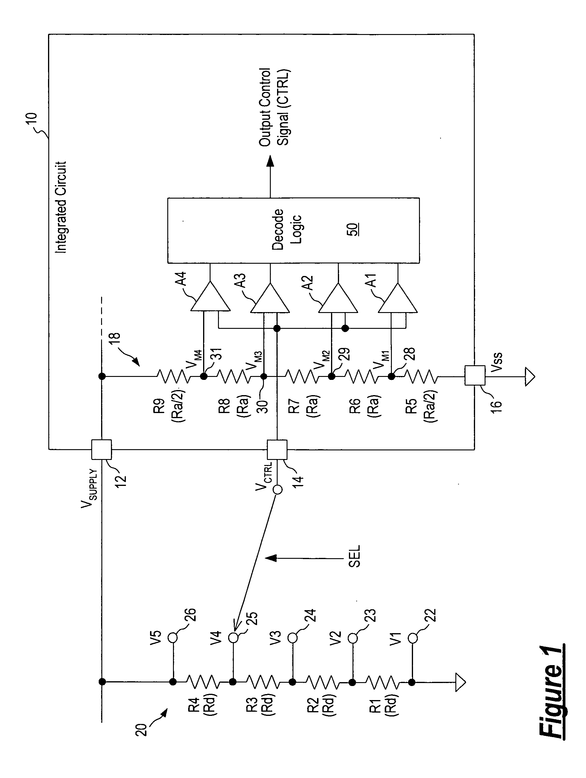
[0021]FIG. 1 is a schematic diagram of an integrated circuit incorporating a control voltage decode circuit and coupled to receive an applied input control voltage according to the present invention. Referring to FIG. 1, an integrated circuit 10 includes a first power supply terminal 12 for receiving a positive power supply voltage VSUPPLY and a second power supply terminal 16 for receiving a negative power supply voltage VSS. Integrated circuit 10 has multiple user selectable operating modes. Each operating mode is associated with a digital state and an output control signal CTRL is used to address or select one of the multiple digital states of integrated circuit 10. In most cases, output control signal CTRL is an n-bit address signal where the number of possible programmable digital states is 2n.
[0022] In integrated circuit 10, the desired digital state is selected by coupling a control pin 14 to a desired programming voltage. Control pin 14 is assigned to more than two digital s...
second embodiment
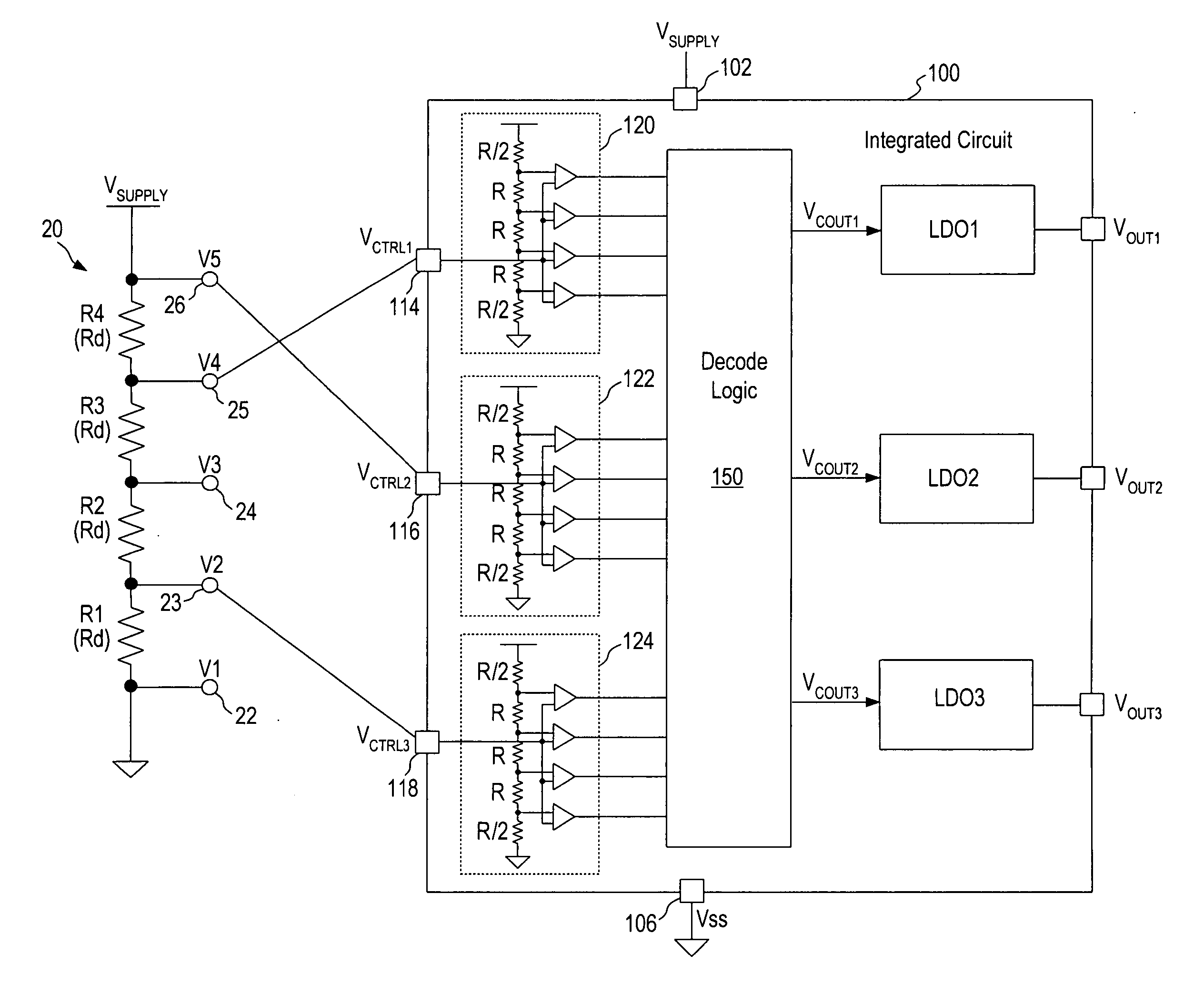
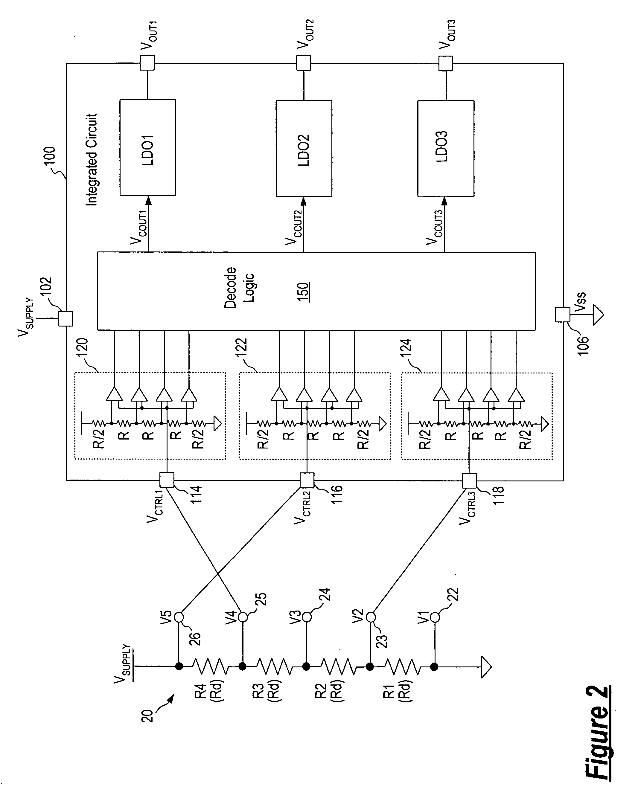
[0035] In the embodiment shown in FIG. 1, the integrated circuit programming circuit and method of the present invention are applied to provide programming of a single control pin. The integrated circuit programming circuit and method can be advantageously applied to the programming of multiple control pins where only a single external voltage divider is required for providing control voltages for all of the control pins to be programmed. FIG. 2 is a schematic diagram of an integrated circuit incorporating multiple control pins coupled to receive a set of applied input control voltages according to the present invention. Referring to FIG. 2, integrated circuit 100 is illustrated as a triple LDO device including three LDO (low-voltage dropout) circuits (LDO1, LDO2 and LDO3) providing three separate output voltages VOUT1, VOUT2, and VOUT3. Each LDO circuit is individually programmed via a control voltage signal (VCOUT1, VCOUT2 or VCOUT3) provided to each LDO circuit to select a desire...
third embodiment
[0043]FIG. 3 is a schematic diagram of an integrated circuit incorporating a control voltage decode circuit with a power-down circuit according to the present invention. Referring to FIG. 3, integrated circuit 200 is constructed in a similar manner as integrated circuit 100 of FIG. 2 except for an on-chip power-up control circuit 280. Specifically, power-up control circuit 280 is connected to the positive power supply voltage terminal 202 receiving the power supply voltage VSUPPLY. Power-up control circuit 280 determines when power is to be provided to the external voltage divider 20 (through terminal 260), when power is provided to the ADC circuits 220, 222 and 224 (through power bus 262), and when power is to be provided to the decode logic circuit 250 (through power bus 264). Power-up control circuit 280 also provides a Latch Data signal on a bus 266 to the decode logic circuit 250 to instruct the decode logic circuit 250 to latch and store the currently decoded data.
[0044] In op...
PUM
 Abstract
Description
Claims
Application Information