Method of feedback control of esc voltage using wafer voltage measurement at the bias supply output

a technology of esc voltage and bias supply, which is applied in the direction of mechanical equipment, variable capacitors, manufacturing tools, etc., can solve the problems of insufficient clamping voltage, risk of damaging the circuit features formed on the wafer surface, and current passing through the wafer, so as to achieve the effect of minimizing the differen

Inactive Publication Date: 2007-06-07
APPLIED MATERIALS INC
View PDF99 Cites 33 Cited by
  • Summary
  • Abstract
  • Description
  • Claims
  • Application Information

AI Technical Summary

Benefits of technology

[0006] In a plasma reactor having an electrostatic chuck (ESC) supporting a wafer to be processed, a method of processing the wafer while controlling an ESC clamping voltage includes applying RF bias power to the ESC from a bias power source at an input to the ESC and applying a D.C. voltage at the input to the ESC from a D.C. voltage source. The voltage and current is measured near the input to produce a measured voltage and a measured current. A wafer voltage signal is provided as a sum of the measured voltage and the measured current multiplied by first and second coefficients respectively, the wafer voltage signal representing the voltage on a wafer supported on the ESC. The method further includes computing a wafer clamping voltage as a difference between a D.C. component of the wafer voltage signal and the D.C. voltage from the D.C. voltage source, and controlling the D.C. voltage to regulate the wafer clamping voltage. In one embodiment, controlling the D.C. voltage is performed so as to minimize a difference between the wafer clamping voltage and a target clamping voltage.

Problems solved by technology

An insufficient clamping voltage would allow the wafer to pop off of the ESC.
An excessive clamping voltage would increase the current through the wafer to a level that risks damaging the circuit features formed on the wafer surface.
An error in wafer voltage measurement may lead to wafer pop off or to excessive ESC-wafer current.
However, the wafer temperature range is limited because the clamping voltage cannot closely approach the upper limit (above which the wafer current is excessive) or the lower limit (below which the wafer may pop off the ESC), without more accurate determination of wafer voltage.
Current methods for estimating wafer voltage tend to be inaccurate, so that the clamping voltage range must be limited to ensure that wafer voltage measurement errors do not cause the clamping voltage to violate the upper and lower limits.
This method is inaccurate when more than one bias frequency is present.
A large error in wafer voltage measurement occurs when such a dual frequency bias is employed.
We have found that the error in the wafer voltage measurement in such a case can create a clamping voltage error exceeding the capacity of the ESC's D.C. voltage supply.

Method used


Image

  • Method of feedback control of esc voltage using wafer voltage measurement at the bias supply output
  • Method of feedback control of esc voltage using wafer voltage measurement at the bias supply output
  • Method of feedback control of esc voltage using wafer voltage measurement at the bias supply output

Examples


Embodiment Construction

ESC With High Contact Force Wafer Cooling:

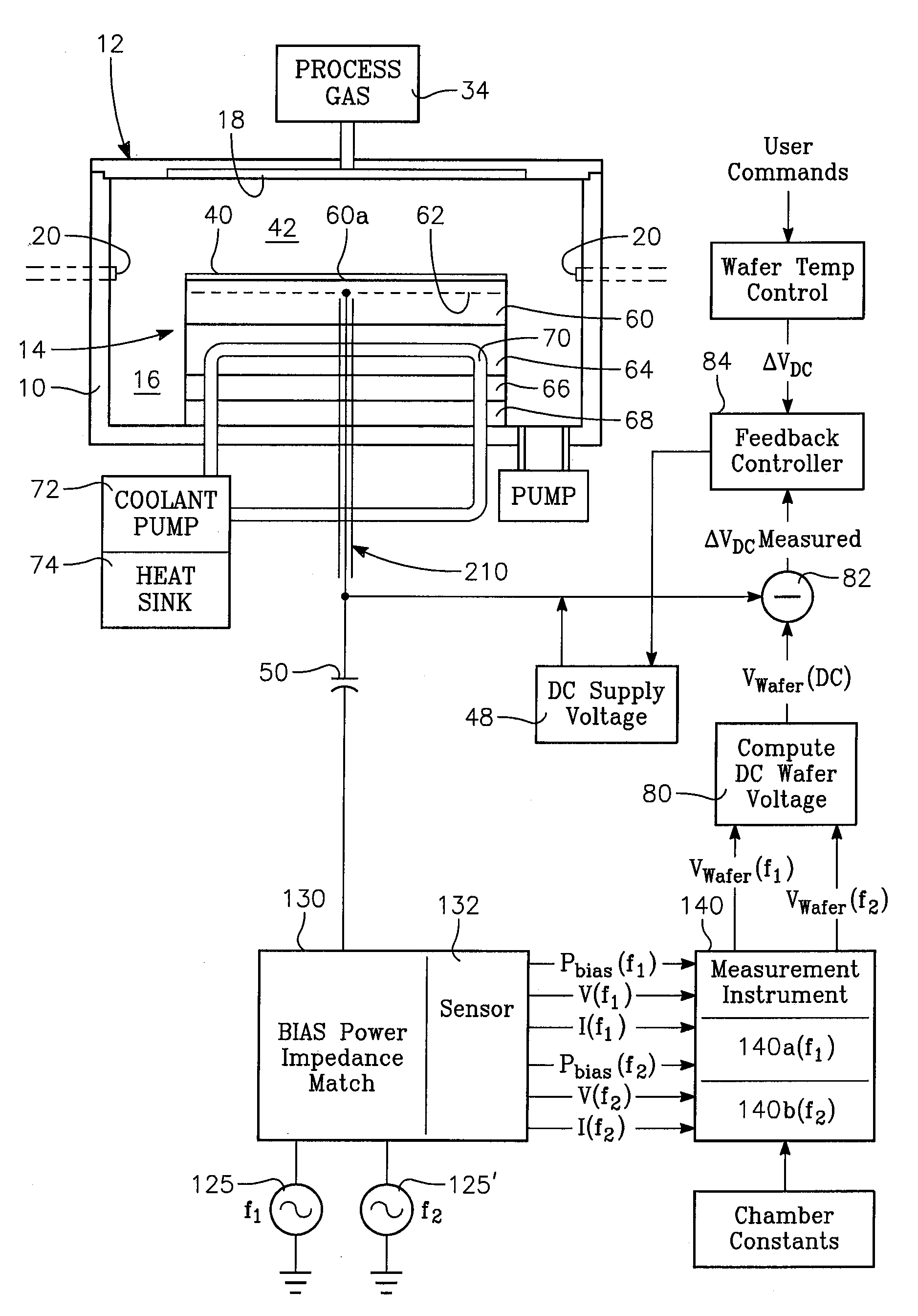
[0024]FIG. 1A illustrates a plasma reactor having a cylindrical side wall 10, a ceiling 12 and a wafer contact-cooling electrostatic chuck (ESC) 14. A pumping annulus 16 is defined between the chuck 14 and the sidewall 10. While the wafer contact-cooling electrostatic chuck 14 may be used in any type of plasma reactor or other reactor (such as thermal process reactor), the reactor in the example of FIG. 1A is of the type in which process gases can be introduced through a gas distribution plate 18 (or “showerhead”) forming a large portion of the ceiling 12. Alternatively, the reactor could have gas distribution inlets 20 (dashed lines) that are separate from the ceiling 12. While the wafer contact-cooling electrostatic chuck 14 may be employed in conjunction with any plasma source (not illustrated in the drawing), such as an inductively coupled RF plasma source, a capacitively coupled RF plasma source or a microwave plasma source, or a torroi...


PUM

PropertyMeasurementUnit
frequencyaaaaaaaaaa
dielectric constantaaaaaaaaaa
pressureaaaaaaaaaa

Abstract

In a plasma reactor having an electrostatic chuck, wafer voltage is determined from RF measurements at the bias input using previously determined constants based upon transmission line properties of the bias input, and this wafer voltage is used to accurately control the DC wafer clamping voltage.

Description

CROSS-REFERENCE TO RELATED APPLICATIONS [0001] This application is a divisional of U.S. patent application Ser. No. 11 / 127,036, filed May 10, 2005 entitled DUAL BIAS FREQUENCY WITH FEEDBACK CONTROL OF E.S.C. VOLTAGE USING WAFER VOLTAGE MEASUREMENT AT THE BIAS SUPPLY OUTPUT by Jang Gyoo Yang, et al. and assigned to the present assignee.BACKGROUND OF THE INVENTION [0002] A plasma reactor for processing a semiconductor wafer typically holds the wafer inside the reactor chamber using an electrostatic chuck (ESC). Plasma ion energy at the wafer surface is controlled by applying a bias voltage to the wafer through the ESC. The ESC essentially consists of an insulator layer having a top surface for supporting the wafer. An electrode or conductive mesh inside the insulator layer beneath the wafer receives a D.C. voltage, creating a voltage drop across the insulator layer between the electrode and the wafer, which produces an electrostatic force clamping the wafer to the ESC. The clamping fo...

Claims


Application Information

Patent Timeline
Patent Type & Authority Applications(United States)
IPC IPC(8): H01T23/00
CPCH01J37/32706Y10T279/23H01L21/6833H01J37/32935
Inventor YANG, JANG GYOOHOFFMAN, DANIEL J.SHANNON, STEVEN C.BURNS, DOUGLAS H.LEE, WONSEOKKIM, KWANG-SOO
Owner APPLIED MATERIALS INC
Why Eureka
Try Eureka