Non-destructive evaluation of microstructure and interface roughness of electrically conducting lines in semiconductor integrated circuits in deep sub-micron regime

a semiconductor integrated circuit and microstructure technology, applied in the field of non-destructive evaluation of electrically conducting lines in semiconductor integrated circuits in deep sub-micron regime, can solve the problems of reducing the effect of geometries, degrading the benefit of small rc delay provided by cu and low-k insulation layers, and no simple, non-destructive methodology available to monitor integrated line surface. , the effect of reducing the cross-section size and reducing the thickness

Inactive Publication Date: 2007-06-07
GLOBALFOUNDRIES INC
View PDF2 Cites 6 Cited by
  • Summary
  • Abstract
  • Description
  • Claims
  • Application Information

AI Technical Summary

Problems solved by technology

While advances in development of integrated circuits continue to lead to higher conductivity Cu and lower effective dielectric constant (k) insulation layer, the size effect in reduced geometries can degrade the benefit of small RC delay provided by Cu and low-k insulation layers.
Presently, there is no any simple, non-destructive methodology available to monitor integrated line surface quality and grain size / boundary configuration for manufacture process monitoring, in-line characterization, or reliability pre-screening.

Method used


Image

  • Non-destructive evaluation of microstructure and interface roughness of electrically conducting lines in semiconductor integrated circuits in deep sub-micron regime
  • Non-destructive evaluation of microstructure and interface roughness of electrically conducting lines in semiconductor integrated circuits in deep sub-micron regime
  • Non-destructive evaluation of microstructure and interface roughness of electrically conducting lines in semiconductor integrated circuits in deep sub-micron regime

Examples


Embodiment Construction

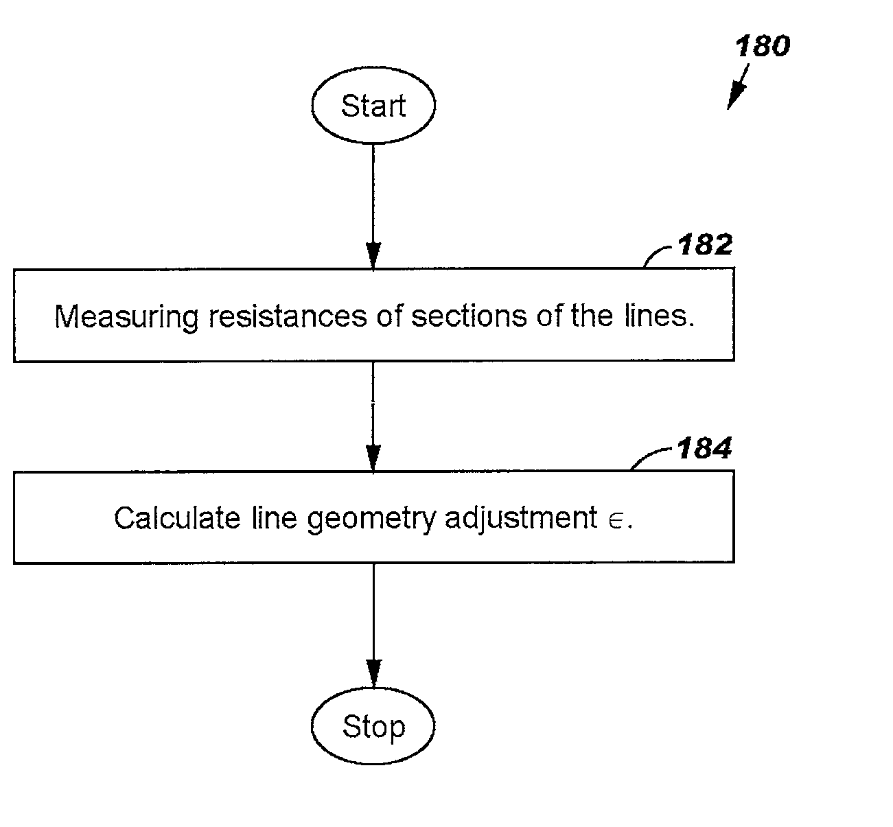
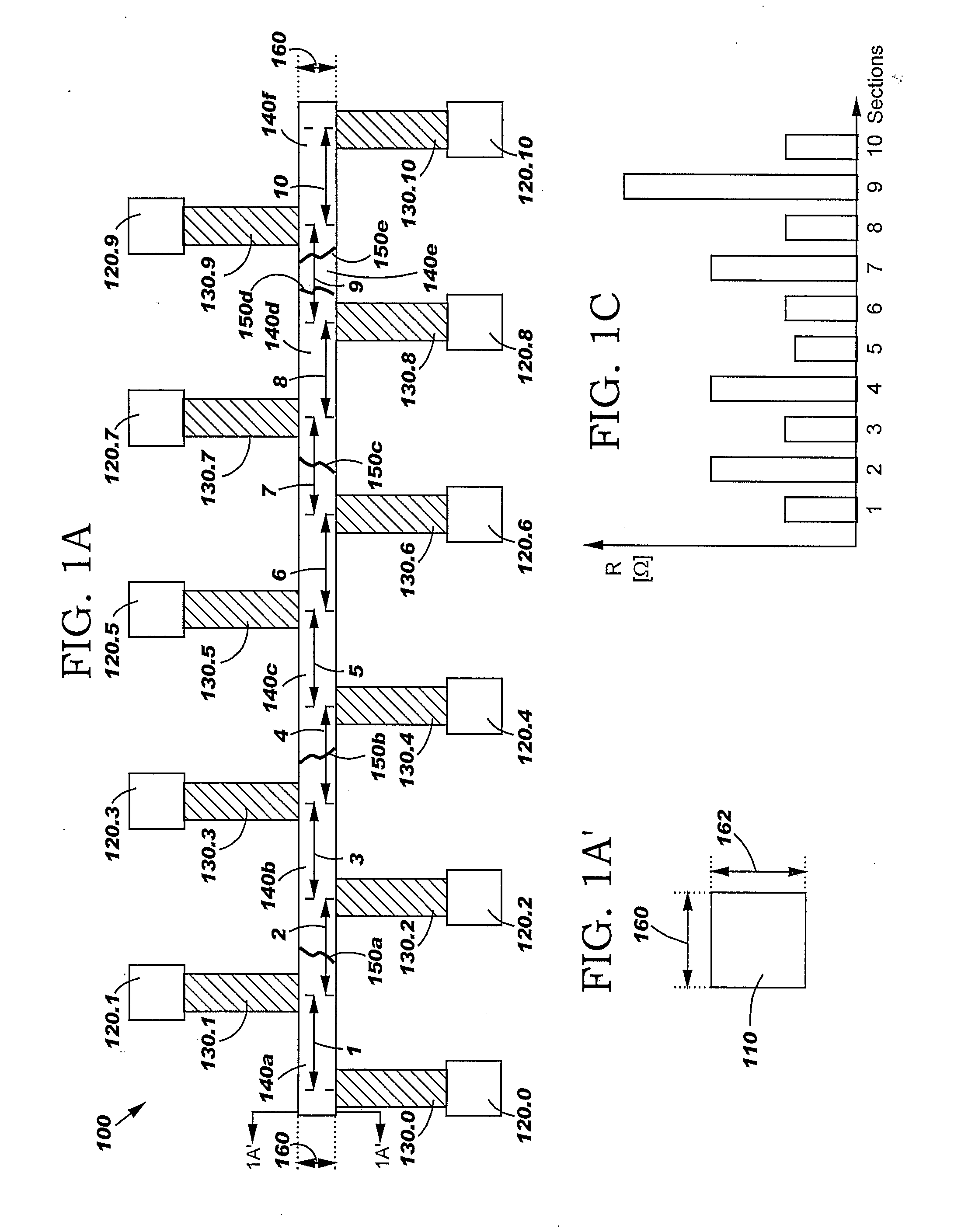
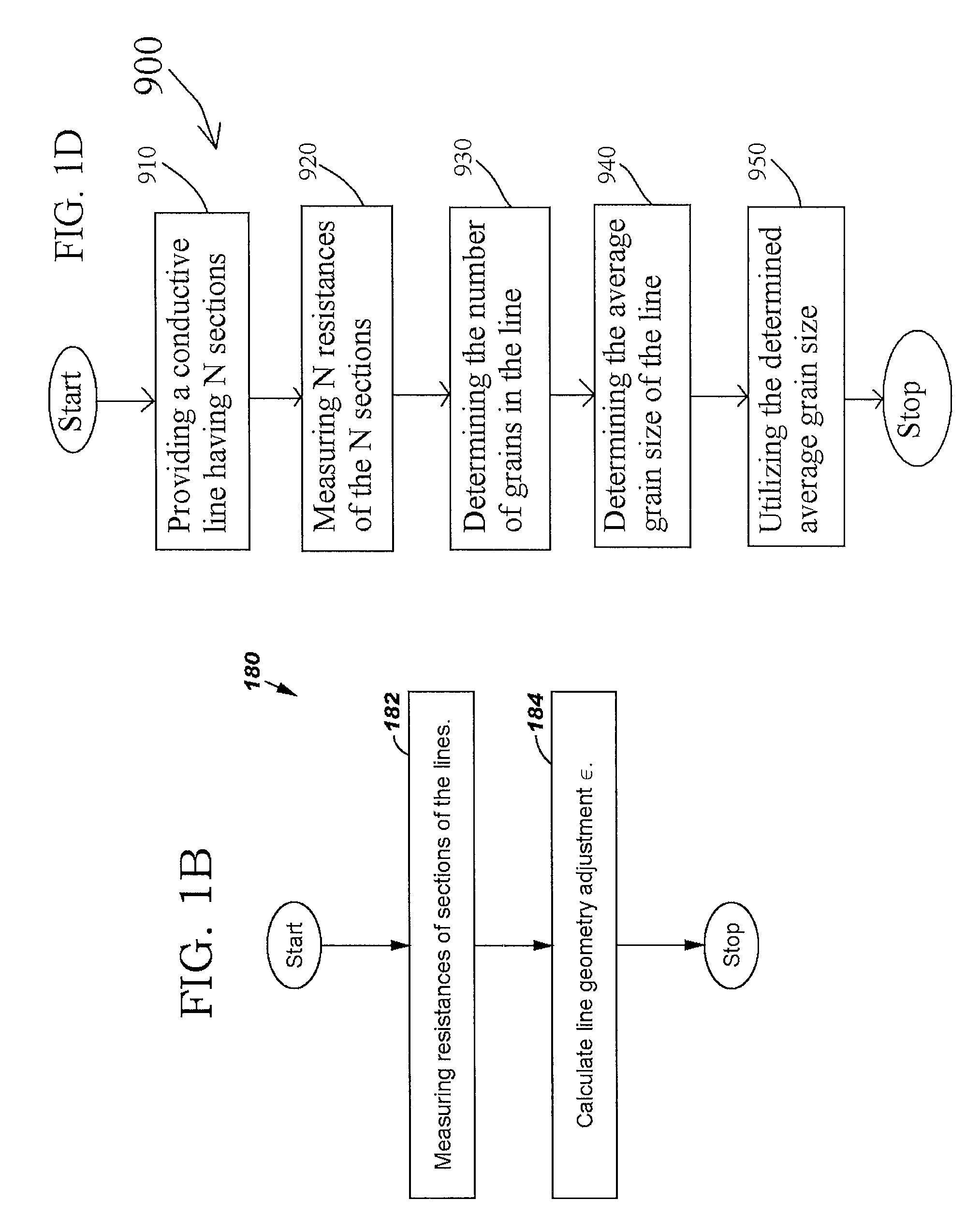
[0013]FIG. 1A shows a top view of a macro 100 comprising a conducting line 110 used for (a) determining line geometry adjustment ε for the macro 100 due to grain boundary electrical resistance and (b) estimating the average grain size of the grains of the line 110, in accordance with embodiments of the present invention. More specifically, the line geometry adjustment ε represents an effective reduction of cross-section size (thickness and line width) of a line as a result of grain boundary electrical resistance.

[0014] In one embodiment, for illustration, the macro 100 can comprise the conducting line 110, eleven pads 120.0-120.10 (collectively referred to as pads 120) and eleven coupling lines 130.0-130.10 (collectively referred to as coupling lines 130) that electrically couple the pads 120 to the line 110. More specifically, the coupling line 130.i electrically couples the pad 120.i to the line 110, wherein i=0-10. In one embodiment, the points at which the 11 coupling lines 130...


PUM


Abstract

Novel structures and methods for evaluating lines in semiconductor integrated circuits. A first plurality of lines are formed on a wafer each of which includes multiple line sections. All the line sections are of the same length. The electrical resistances of the line sections are measured. Then, a first line geometry adjustment is determined based on the electrical resistances of all the sections. The first line geometry adjustment represents an effective reduction of cross-section size of the lines due to grain boundary electrical resistance. A second plurality of lines of same length and thickness can be formed on the same wafer. Then, second and third line geometry adjustments are determined based on the electrical resistances of these lines measured at different temperatures. The second and third line geometry adjustments represent an effective reduction of cross-section size of the lines due to grain boundary electrical resistance and line surface roughness.

Description

[0001] This application is a divisional of Ser. No. 10 / 711,418, filed Sep. 17, 2004.BACKGROUND OF THE INVENTION [0002] 1. Technical Field [0003] The present invention relates to semiconductor integrated circuits, and more particularly, to the non-destructive evaluation of electrically conducting lines in semiconductor integrated circuits. [0004] 2. Related Art [0005] As dimensions reach the deep-submicron level on the order of the mean-free path of electrons of Cu interconnect wires, the size effect on the resistivity of Cu interconnects corresponding to reductions of wire dimensions becomes more significant. While advances in development of integrated circuits continue to lead to higher conductivity Cu and lower effective dielectric constant (k) insulation layer, the size effect in reduced geometries can degrade the benefit of small RC delay provided by Cu and low-k insulation layers. Three types of extra electron scattering mechanisms due to the size effect in addition to the isot...

Claims


Application Information

Patent Timeline
Patent Type & Authority Applications(United States)
IPC IPC(8): G06F17/50
CPCH01L22/34H01L2924/0002H01L2924/00
Inventor CHEN, FENGAMBINO, JEFFREY P.GILL, JASON P.LI, BAOZHENSULLIVAN, TIMOTHY D.
Owner GLOBALFOUNDRIES INC
Why Eureka
Try Eureka