Radiation detecting apparatus and radiation imaging system using the same
- Summary
- Abstract
- Description
- Claims
- Application Information
AI Technical Summary
Benefits of technology
Problems solved by technology
Method used
Image

Examples
first embodiment
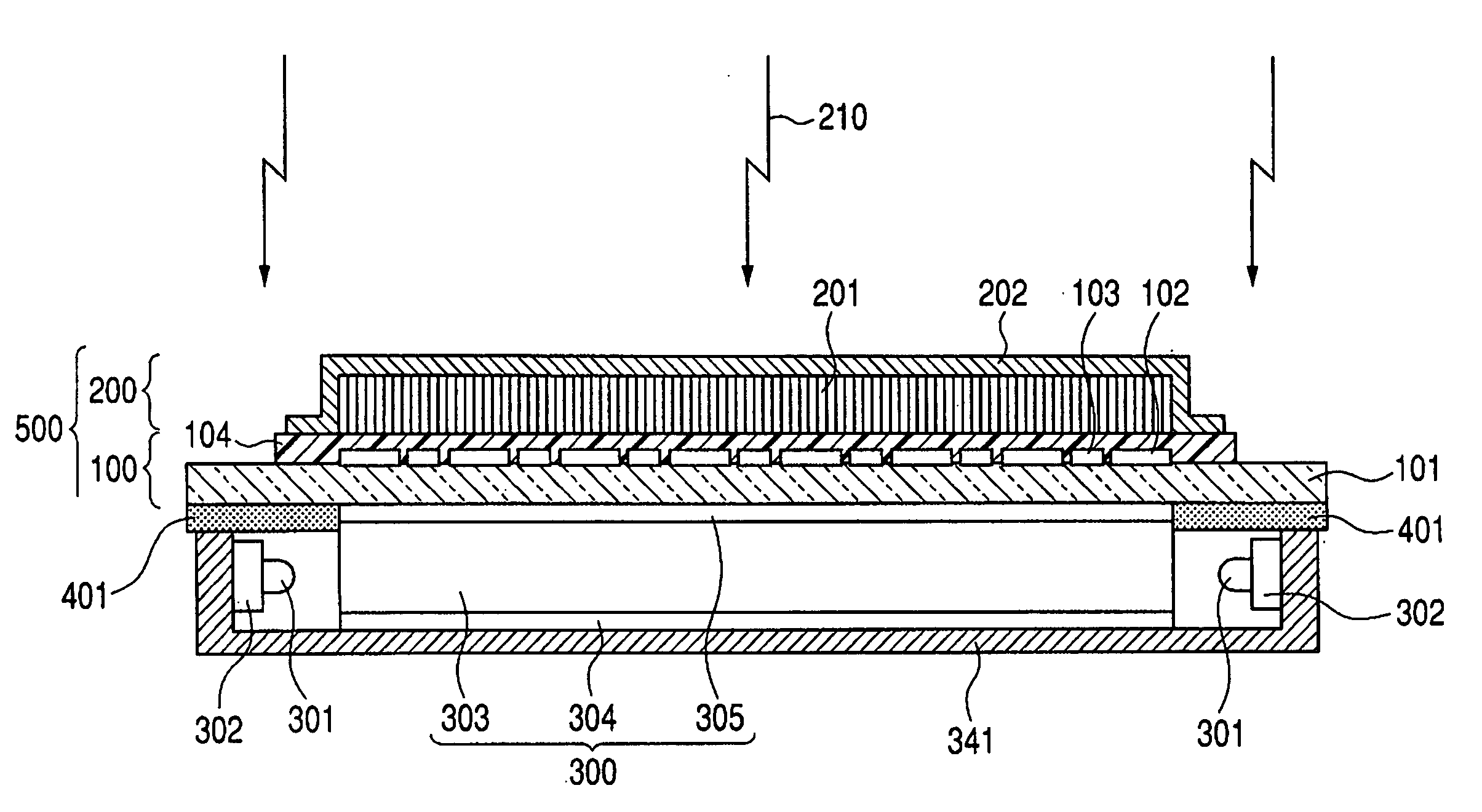
[0040]FIG. 1 is a sectional view showing a first embodiment of a radiation detecting apparatus according to the present invention. The present embodiment is of an indirect type. In the Figure, reference numeral 200 denotes a wavelength conversion portion configured by a phosphor 201 comprising CsI:TI and the like and a protection layer 202.
[0041] Further, reference numeral 100 denotes a photoelectrical conversion panel, which is configured by a plurality of photoelectrical conversion elements 102, a plurality of switch elements 103, an insulating protection layer 104, and a transparent insulating substrate 101. By this wavelength conversion portion 200 and the photoelectric conversion panel 100, an indirect type radiation detecting panel 500 is configured. Incidentally, since the indirect type radiation detecting panel 500 is publicly known, the detailed description thereof will be omitted.
[0042] The bottom of the indirect type radiation detecting panel 500 is provided with light ...
second embodiment
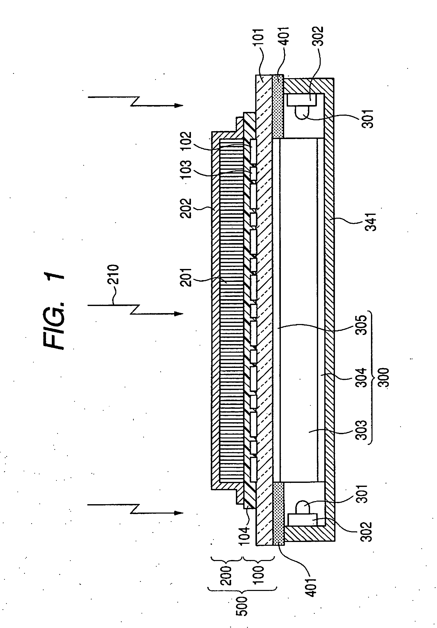
[0047]FIG. 2 is a sectional view showing a second embodiment of the present invention. In FIG. 2, the same reference numerals are attached to the same parts as FIG. 1. The present embodiment is also of an indirect type.
[0048] In the present embodiment, similarly to FIG. 1, by light guiding means 300 comprising a light guiding plate 303, a reflecting plate 304, and a diffusing plate 305, a light of an LED 301 disposed at its side portion is guided to the entirety of an photoelectric conversion element 102 or a switch element 103 or a phosphor 201 of a radiation detecting panel 500. The LED 301, similarly to FIG. 1, is plurally disposed in a transverse direction (front and back directions in the Figure).
[0049] A shielding electrical mounting substrate 402 mounting the LED 301 is attached to an upper transparent insulating substrate 101. The shielding electrical mounting substrate 402, for example, is made from a stainless or molybdenum plate, and the like, and absorbs a radiation 21...
third embodiment
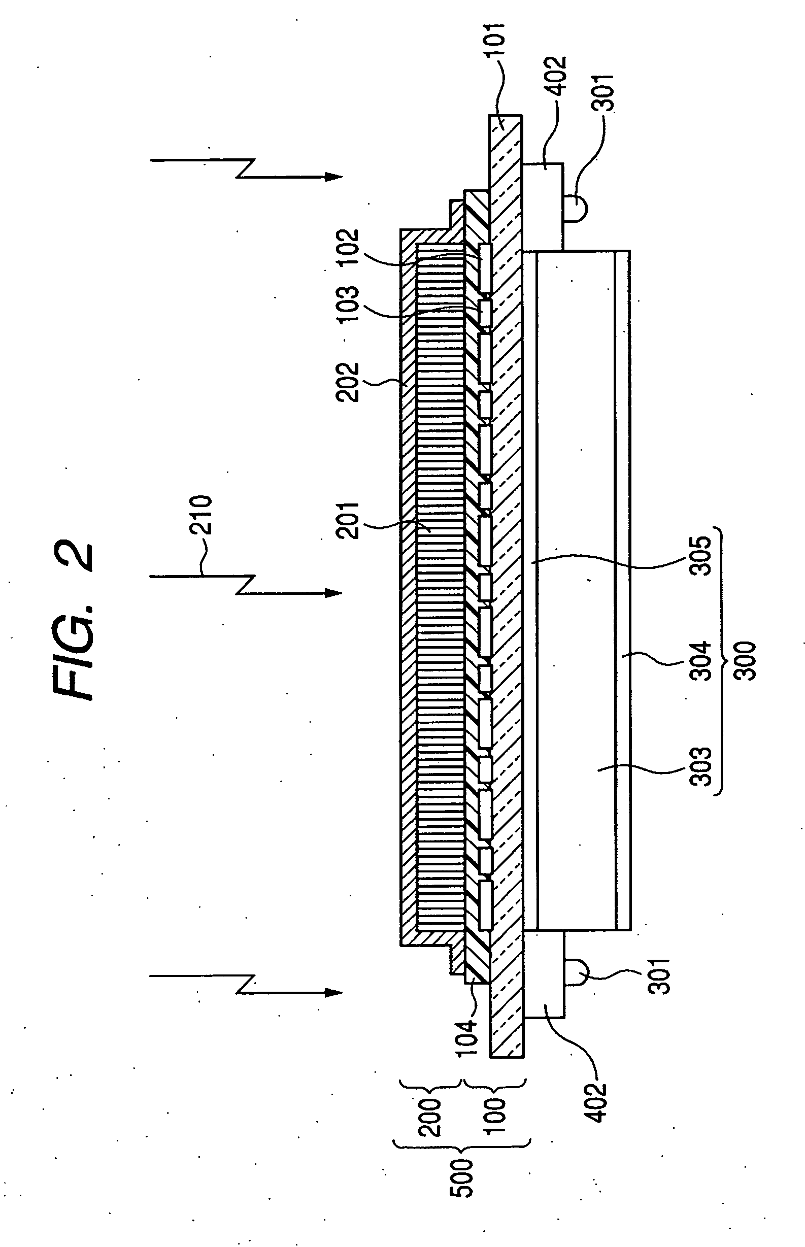
[0052]FIG. 3 is a sectional view showing a third embodiment of the present invention. The present embodiment also is of an indirect type. In FIG. 3, the same parts as those of FIGS. 1 and 2 are attached with the same reference numerals. A shielding plate 403 is installed at a part of a cover 351 covering the periphery of a radiation detecting apparatus. The shielding plate 403, similarly to FIG. 1, is made from a stainless or molybdenum plate and the like, and absorbs a radiation 210 from the upper radiation source, and reduces the radiation 210 incident in the direction of an LED, thereby inhibiting radiation damages of the LED.
[0053] In the present embodiment, though a structure of attaching the shielding plate 403 on the cover 351 is shown in a representative manner, even if the shielding plate 403 is attached to a grid or a protection plate and the like provided that it is an exterior part of the radiation detecting apparatus, this does not deviate from the scope of the present...
PUM
 Abstract
Description
Claims
Application Information