Self-standing GaN single crystal substrate, method of making same, and method of making a nitride semiconductor device

a self-standing, single crystal substrate technology, applied in semiconductor/solid-state device manufacturing, semiconductor devices, electrical equipment, etc., can solve the problems of deterioration of the characteristics short lifetime, and the method has a number of crystal defects, so as to improve the non-defective product yield of the nitride semiconductor device, reduce the warping of the gan self-standing substrate, and improve the degree of contact

Inactive Publication Date: 2007-06-14
HITACHI CABLE
View PDF9 Cites 77 Cited by
  • Summary
  • Abstract
  • Description
  • Claims
  • Application Information

AI Technical Summary

Benefits of technology

[0031] In accordance with the invention, the self-standing GaN single crystal substrate can enhance the non-defective product yield of a nitr...

Problems solved by technology

The nitride semiconductor devices obtained by the above growth method have a number of crystal defects therein.
The crystal defect can cause deterioration in characteristics of the nitride semiconductor device or short lifetime thereof.
The GaN self-standing substrate thus made has still a number of defects.
When a nitride semiconductor d...

Method used


Image

  • Self-standing GaN single crystal substrate, method of making same, and method of making a nitride semiconductor device
  • Self-standing GaN single crystal substrate, method of making same, and method of making a nitride semiconductor device
  • Self-standing GaN single crystal substrate, method of making same, and method of making a nitride semiconductor device

Examples


examples 1-3

[0060] Examples 1-3 according to the invention will be described below. However, the invention is not limited to these.

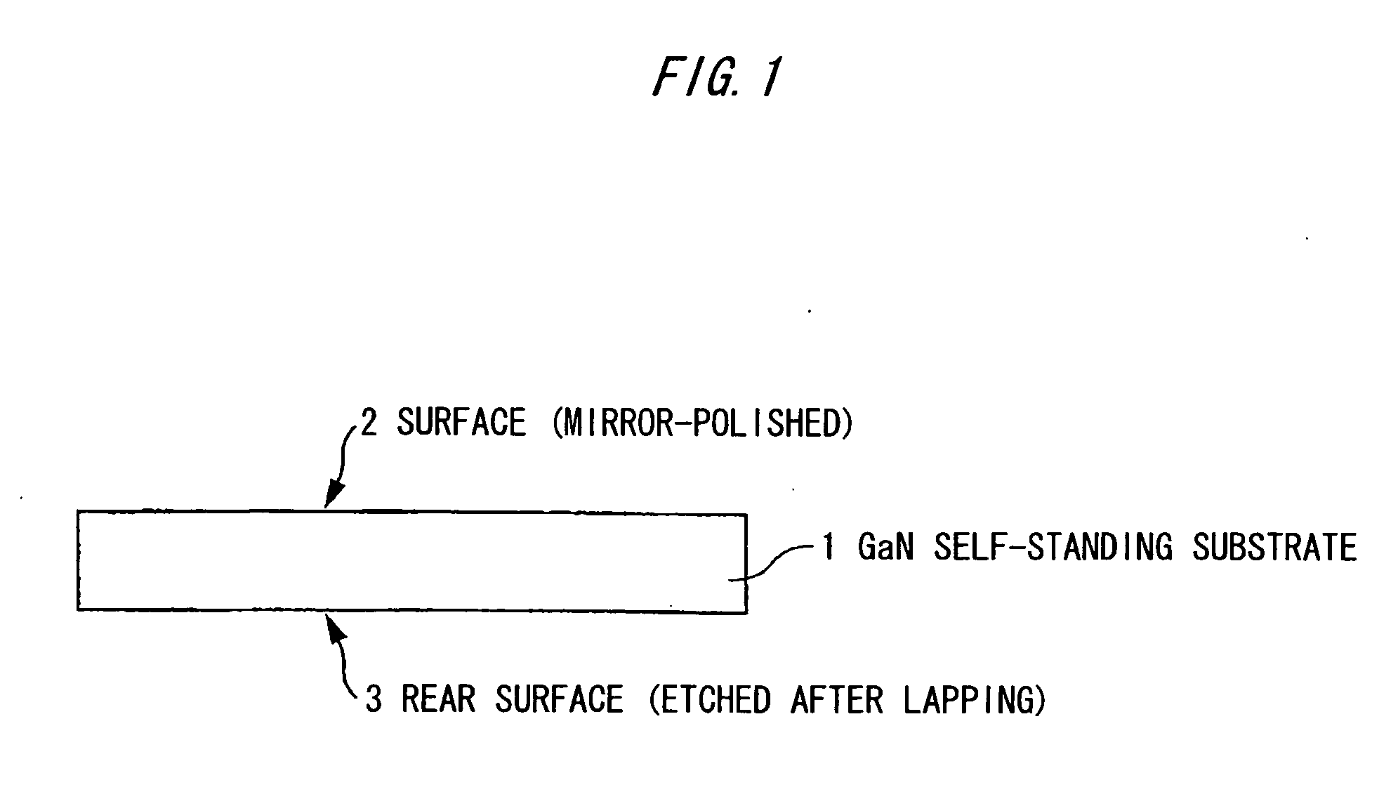
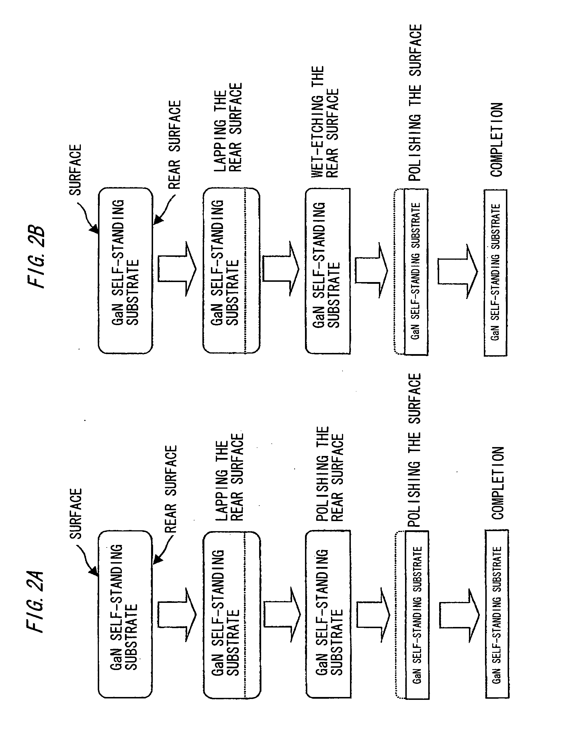
[0061] By using the method of making the GaN self-standing substrate in the embodiment (as shown in FIG. 2B), GaN self-standing substrates are made such that the surface thereof is mirror-polished and the rear surface is treated to be 1 micrometer (=Example 1), 7 micrometers (=Example 2), and 10 micrometers (=Example 3) in arithmetic mean roughness Ra.

[0062] In detail, after the GaN self-standing substrate is separated from the sapphire substrate and the rear surface thereof is lapped (with GC #800), the rear surface of the GaN self-standing substrate is polished by etching while being soaked into 1 N NaOH aqueous solution. In this case, the soak time (etch time) in NaOH aqueous solution is adjusted to be 10 min, 30 min and 60 min such that the arithmetic mean roughness Ra of the rear surface of the GaN self-standing substrate is to be 1 micrometer, 7 micrometers ...


PUM


Abstract

A self-standing gallium nitride-based semiconductor single crystal substrate has a surface (Ga-face) mirror-polished, and a rear surface (N-face) having an arithmetic mean roughness Ra of 1 micrometer or more and 10 micrometers or less. A nitride semiconductor device is fabricated such that, before the gallium nitride-based semiconductor single crystal substrate is attached to a substrate holder of a vapor phase growth apparatus, the substrate is adjusted such that its rear surface (N-face) has a arithmetic mean roughness Ra to be in face-to-face contact with the substrate holder.

Description

[0001] The present application is based on Japanese patent application No. 2005-354454, the entire contents of which are incorporated herein by reference. BACKGROUND OF THE INVENTION [0002] 1. Field of the Invention [0003] This invention relates to a self-standing GaN-based single crystal substrate (herein also called simply GaN self-standing substrate or self-standing GaN single crystal substrate) and, in particular, to a self-standing GaN-based single crystal substrate that can enhance the non-defective product yield of a nitride semiconductor device. Also, this invention relates to a method of making the self-standing GaN-based single crystal substrate and a method of making the nitride semiconductor device by using the self-standing GaN-based single crystal substrate. [0004] 2. Description of the Related Art [0005] Nitride-based semiconductor materials have a wide bandgap and are of direct transition type. Therefore, they are great deal applied to short-wavelength light emitting...

Claims


Application Information

Patent Timeline
IPC IPC(8): H01L31/00H01L33/06H01L33/32
CPCH01L21/02008
Inventor KAWAGUCHI, YUSUKEMEGURO, TAKESHI
Owner HITACHI CABLE
Why Eureka
Try Eureka