Substrate having minimum kerf width

a technology of substrates and substrates, applied in the direction of printed circuit parts, printed circuit manufacture, basic electric elements, etc., to achieve the effect of reducing narrowing the width of the cutting device, and reducing the width between adjoining package outlines

Active Publication Date: 2007-06-14
SANDISK TECH LLC
View PDF16 Cites 17 Cited by
  • Summary
  • Abstract
  • Description
  • Claims
  • Application Information

AI Technical Summary

Benefits of technology

[0015] Having a stepped, diagonal or otherwise discontinuous shaped plating bar provides an advantage that the kerf width between adjoining package outlines may have a thinner width than known in the prior art. First, as it is not necessary to remove the plating bar, the width of the cutting device need not be greater than the width of the plating bar. Second, because portions of the plating bar pass across the boundary between adjoining package outlines, even if the path of the cutting device varies from straight due to engineering tolerances, the cut will still sever the plating bar between adjoining package outlines to isolate the electrical terminals.

Problems solved by technology

Second, because portions of the plating bar pass across the boundary between adjoining package outlines, even if the path of the cutting device varies fro

Method used


Image

  • Substrate having minimum kerf width
  • Substrate having minimum kerf width
  • Substrate having minimum kerf width

Examples


Embodiment Construction

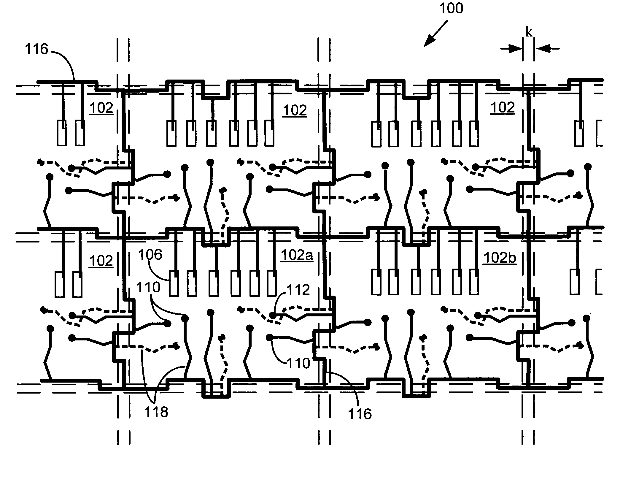
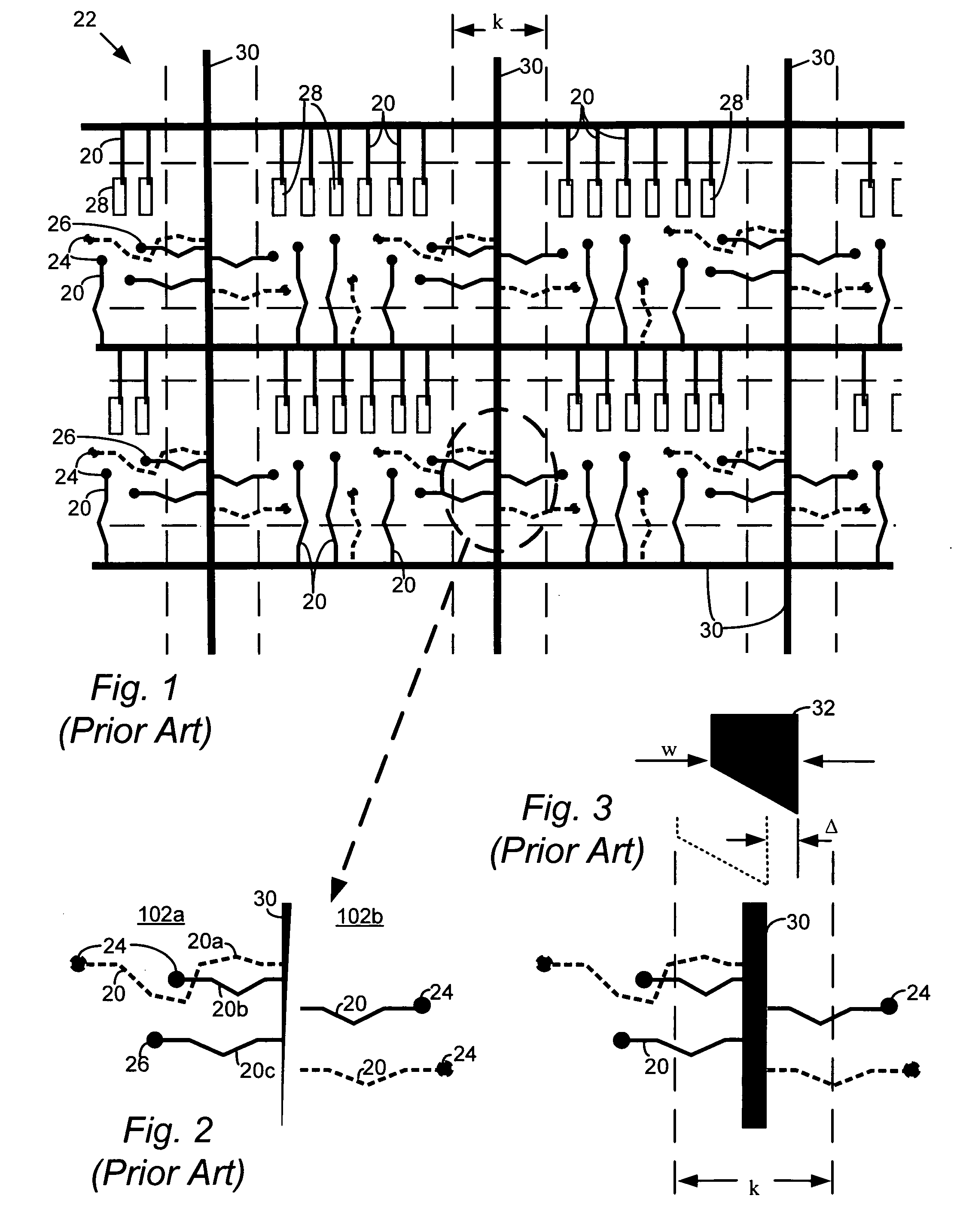
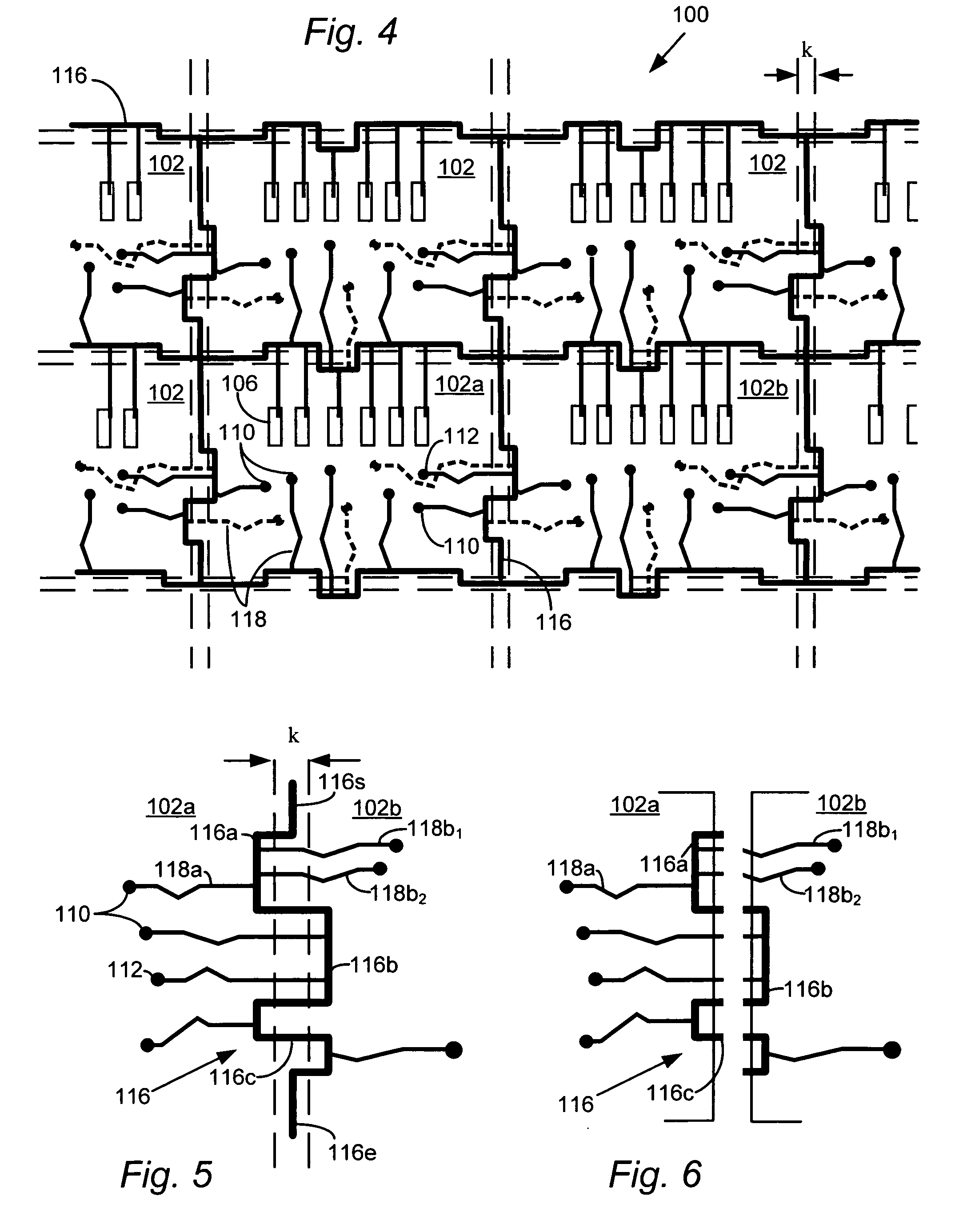
[0033] Embodiments of the invention will now be described with reference to FIGS. 4 through 16, which relate to a semiconductor die substrate including a minimum kerf width cut between adjoining semiconductor package outlines on the panel, while ensuring electrical isolation of plated contacts. It is understood that the present invention may be embodied in many different forms and should not be construed as being limited to the embodiments set forth herein. Rather, these embodiments are provided so that this disclosure will be thorough and complete and will fully convey the invention to those skilled in the art. Indeed, the invention is intended to cover alternatives, modifications and equivalents of these embodiments, which are included within the scope and spirit of the invention as defined by the appended claims. Furthermore, in the following detailed description of the present invention, numerous specific details are set forth in order to provide a thorough understanding of the ...


PUM


Abstract

A semiconductor die substrate panel is disclosed including a minimum kerf width between adjoining semiconductor package outlines on the panel, while ensuring electrical isolation of plated electrical terminals. By reducing the width of a boundary between adjoining package outlines, additional space is gained on a substrate panel for semiconductor packages.

Description

BACKGROUND OF THE INVENTION [0001] 1. Field of the Invention [0002] Embodiments of the present invention relate to a semiconductor die substrate panel including a minimum kerf width between adjoining semiconductor package outlines on the panel, while ensuring electrical isolation of plated contacts. [0003] 2. Description of the Related Art [0004] The strong growth in demand for portable consumer electronics is driving the need for high-capacity storage devices. Non-volatile semiconductor memory devices, such as flash memory storage cards, are becoming widely used to meet the ever-growing demands on digital information storage and exchange. Their portability, versatility and rugged design, along with their high reliability and large capacity, have made such memory devices ideal for use in a wide variety of electronic devices, including for example digital cameras, digital music players, video game consoles, PDAs and cellular telephones. [0005] While a wide variety of packaging config...

Claims


Application Information

Patent Timeline
IPC IPC(8): H01L23/544
CPCH01L21/4846H01L23/49838H01L24/97H01L2924/01029H01L2924/01074H01L2924/01078H01L2924/01079H01L2924/01082H01L2924/14H01L2924/1433H05K3/0052H05K3/242H05K2201/09263H01L2924/01005H01L2924/01006H01L2924/01019H01L2924/01033H01L2924/10253H01L2924/00H01L2924/181
Inventor TAKIAR, HEMWANG, KEN JIAN MINGLIAO, CHIH-CHINCHEN, HAN-SHIAO
Owner SANDISK TECH LLC
Why Eureka
Try Eureka