System memory board subsystem using dram with stacked dedicated high speed point to point links

a memory board and subsystem technology, applied in the field of memory subsystems, can solve the problems of insufficient data rate, undesirable nature of above described latencies, and limited number of dimms which may be utilized, and achieve the effect of efficient utilization of printed circuit board spa

Active Publication Date: 2007-06-14
ORACLE INT CORP
View PDF16 Cites 108 Cited by
  • Summary
  • Abstract
  • Description
  • Claims
  • Application Information

AI Technical Summary

Problems solved by technology

For a variety of reasons, including loading considerations, such designs have been unable to provide sufficiently high data rates when multiple DIMMs are placed on the same data channel.
While the proposed scheme may provide for improvements over prior technologies, the limited number of DIMMs which may be utilized may be seen as undesirable.
In addition, the nature of the above described latencies may also be undesirable.

Method used


Image

  • System memory board subsystem using dram with stacked dedicated high speed point to point links
  • System memory board subsystem using dram with stacked dedicated high speed point to point links
  • System memory board subsystem using dram with stacked dedicated high speed point to point links

Examples


Embodiment Construction

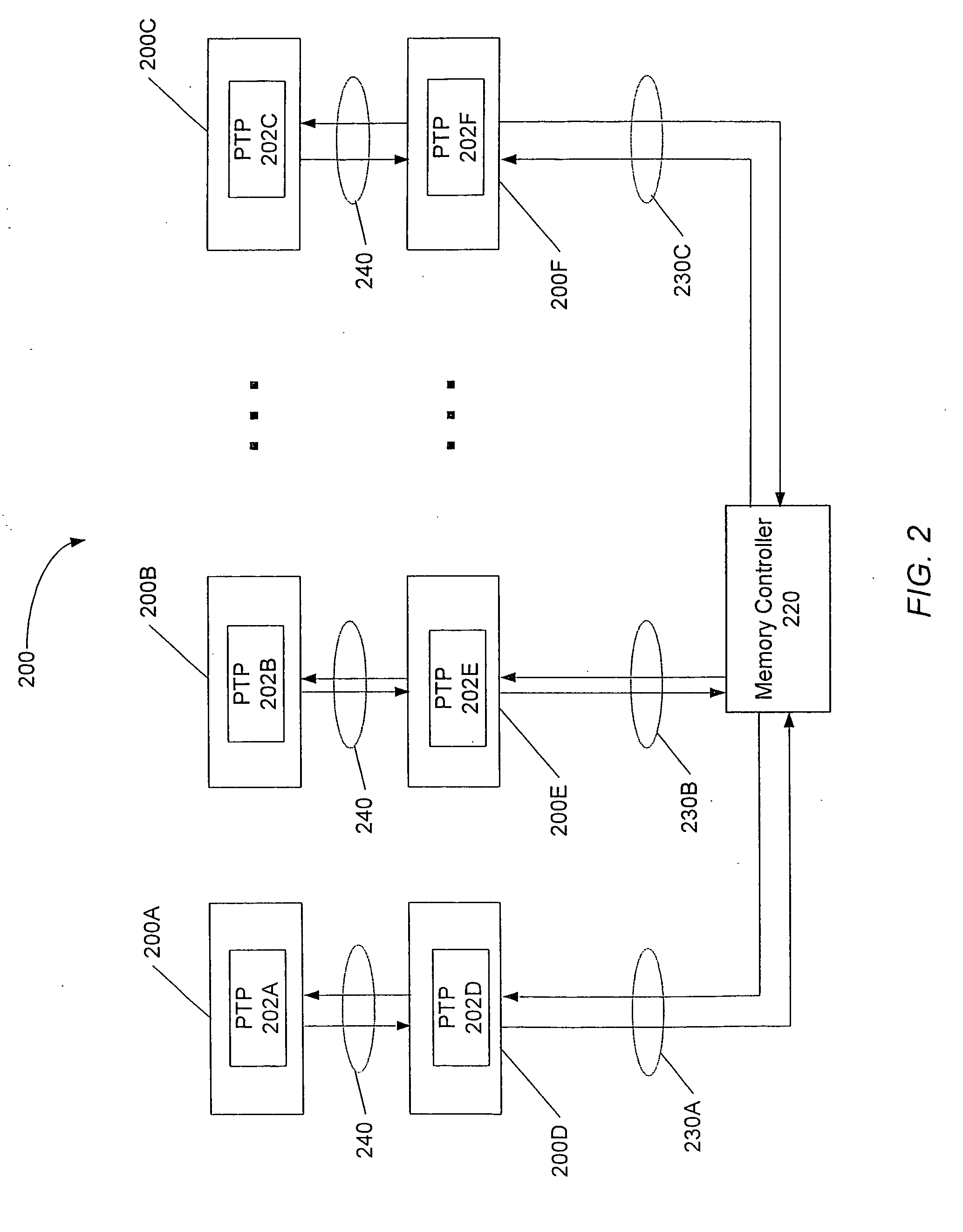
[0029] Turning now to FIG. 2, one embodiment of a memory subsystem is shown. In the example, a memory controller 220, or “host”, is shown coupled to memory modules 200D, 200E, and 200F, via links 230A, 230B, and 230C, respectively. For ease of illustration, FIG. 2 only depicts the memory controller 220 as being directly coupled to three memory modules. However, as noted by the ellipses in FIG. 2, more memory modules than those shown may be coupled to memory controller 220. In one embodiment, memory controller 220 may be directly coupled to sixteen. However, other embodiments may include fewer or greater than sixteen modules. In addition, it is to be understood that the memory controller 220 may comprise one or more chips or devices.

[0030]FIG. 2 also shows each of memory modules 200D-200F to be coupled to further memory modules via links 240. In particular, memory module 200D is coupled to memory module 200A, memory module 200E is coupled to memory module 200B, and memory module 200...


PUM


Abstract

A memory system comprising memory modules including memory chips stacked with switching circuits. A memory controller coupled to the memory modules is configured to initiate memory accesses. When a stacked switching circuit detects the memory access, the switching circuit routes the access to another memory module if the access is not directed to a memory chip of the receiving memory module, or processes the access locally if the access is directed to a memory chip of the receiving memory module. The memory controller and memory modules are coupled via bi-directional serial links. Each memory module may include multiple stacked switching circuits, each of which may be coupled to fewer than all of the memory chips within the memory module. Switching circuits further include circuitry configured to de-serialize data prior to conveyance to a memory chip, and serialize data received from a DRAM chip prior to transmitting the received data. Switching circuits may be coupled to a stacked memory chip via a flexible interconnect, and may also be manufactured side by side with a corresponding memory chip on a flexible circuit board.

Description

BACKGROUND OF THE INVENTION [0001] 1. Field of the Invention [0002] This invention relates to memory subsystems and, more particularly, to the topology of a memory system architecture. [0003] 2. Description of the Related Art [0004] Over the years, demands placed upon computing systems have increased. As demands increase and technology has advanced, efforts have been made to both increase the capacity of memory systems and reduce memory system latencies. In recent years, various proposals have been made, including proposals for fully-buffered dual-inline memory modules (FB-DIMMs). Traditionally, DIMMs have been configured to buffer both addresses and commands, but the data interface itself has been unbuffered. For a variety of reasons, including loading considerations, such designs have been unable to provide sufficiently high data rates when multiple DIMMs are placed on the same data channel. As a result, DIMMs that buffer data (i.e., FB-DIMMS), as well as addresses and commands, h...

Claims


Application Information

Patent Timeline
Patent Type & Authority Applications(United States)
IPC IPC(8): G06F13/00
CPCG06F13/1684G11C5/00
Inventor DOBLAR, DREW G.RISK, GABRIEL C.WU, CHUNG-HSIAO R.
Owner ORACLE INT CORP
Why Eureka
Try Eureka