
MCU/driver point of load digital controller with optimized voltage

a digital controller and point of load technology, applied in the direction of electric variable regulation, process and machine control, instruments, etc., can solve the problems of power loss, high power switched power supply problems, and inability to independently control the dead time of analog controllers, so as to maximize the optimize the operation of power efficiency of switching power converters.

Active Publication Date: 2007-06-21
SILICON LAB INC
View PDF5 Cites 27 Cited by
  • Summary
  • Abstract
  • Description
  • Claims
  • Application Information

AI Technical Summary

Benefits of technology

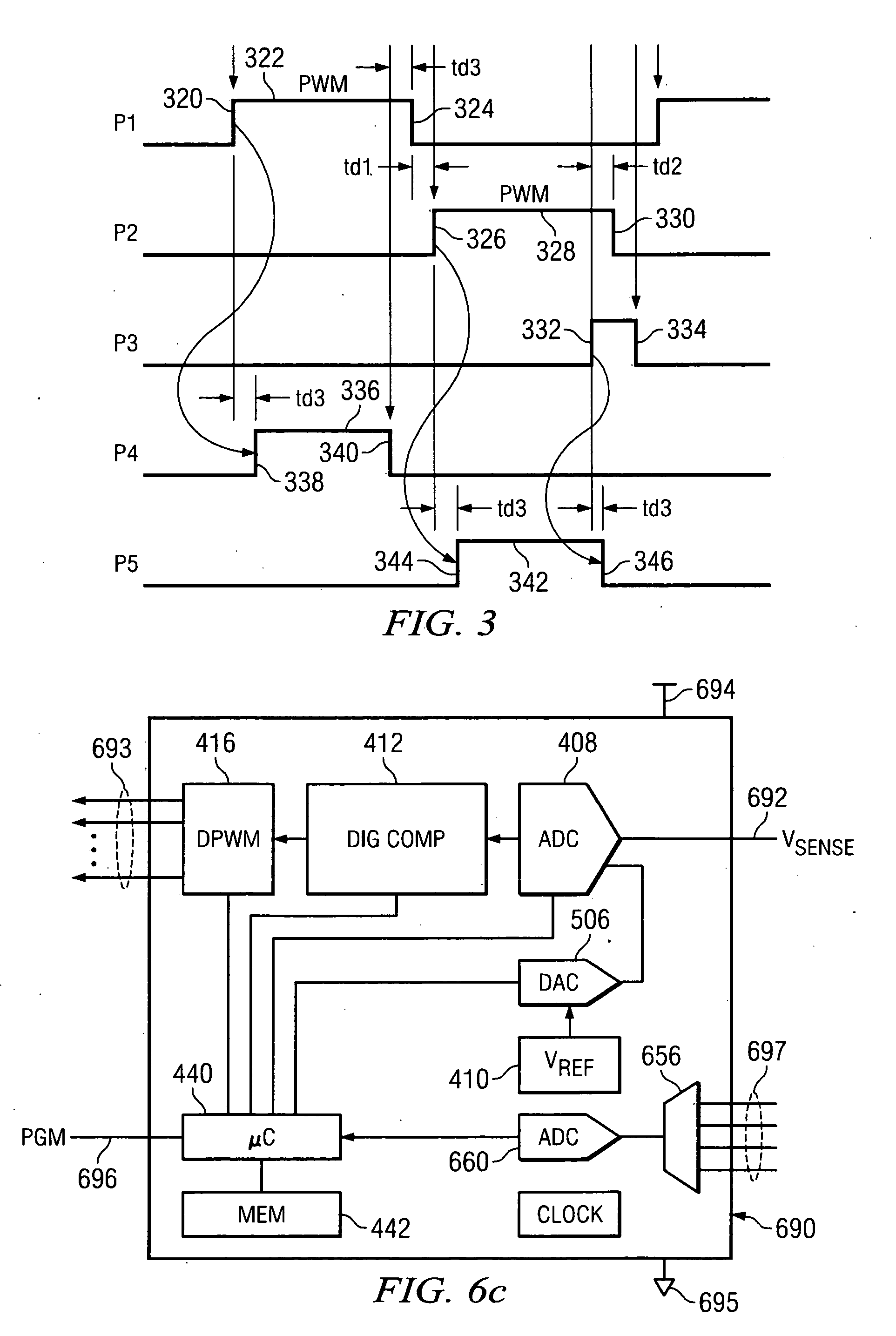
[0008] The present invention disclosed and claimed herein, in one aspect thereof, comprises a system for optimizing power efficiency of a switching power converter operating at a switching frequency. A digital controller receives an analog signal representing an output DC voltage of the switching power converter for comparison to a desired output voltage and generates switching control signals to control the operation of the power supply to regulate the output DC voltage to said desired output voltage. At least two of the switching control signals have a dead time between a first edge of a first control signal and a second edge of a second control signal. The dead time is programmable to control a power efficiency of the switching power converter. The switching control signals further switch the power supply between a continuous conduction mode and a discontinuous conduction mode responsive to a mode control signal. The operation of the digital controller is parameterized by a set of operating parameters. A driver circuit connects to an output of the digital controller to drive the switching control signals and includes an input for a regulated voltage. A voltage regulator selects the regulated voltage to the driver circuit responsive to a voltage control signal. A micro controller determines the parameters used by said digital controller, establishes the programmable dead time between the control signals and generates the mode control signal responsive to a current signal from the switching power converter to substantially maximize the power efficiency of the switching power converter, generate the voltage control signal to the voltage regulator.

Problems solved by technology

Analog controllers do not have the ability to independently control the dead time for control signals for complementary switchers.
High power switched power supplies often have problems when switching between complementary switches of the supply with various power losses.
These power losses can be caused by shoot through currents, body diode conduction, RDS on losses and gate losses within the switches of the switched power supply.

Method used


Image

  • MCU/driver point of load digital controller with optimized voltage
  • MCU/driver point of load digital controller with optimized voltage
  • MCU/driver point of load digital controller with optimized voltage

Examples


Embodiment Construction

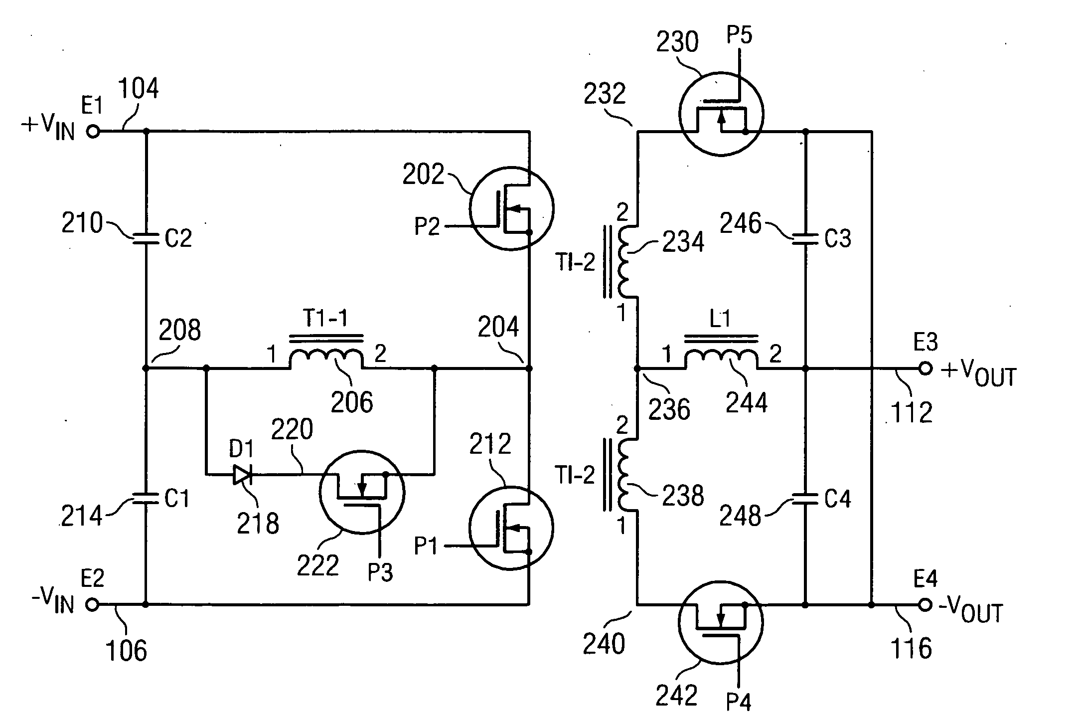
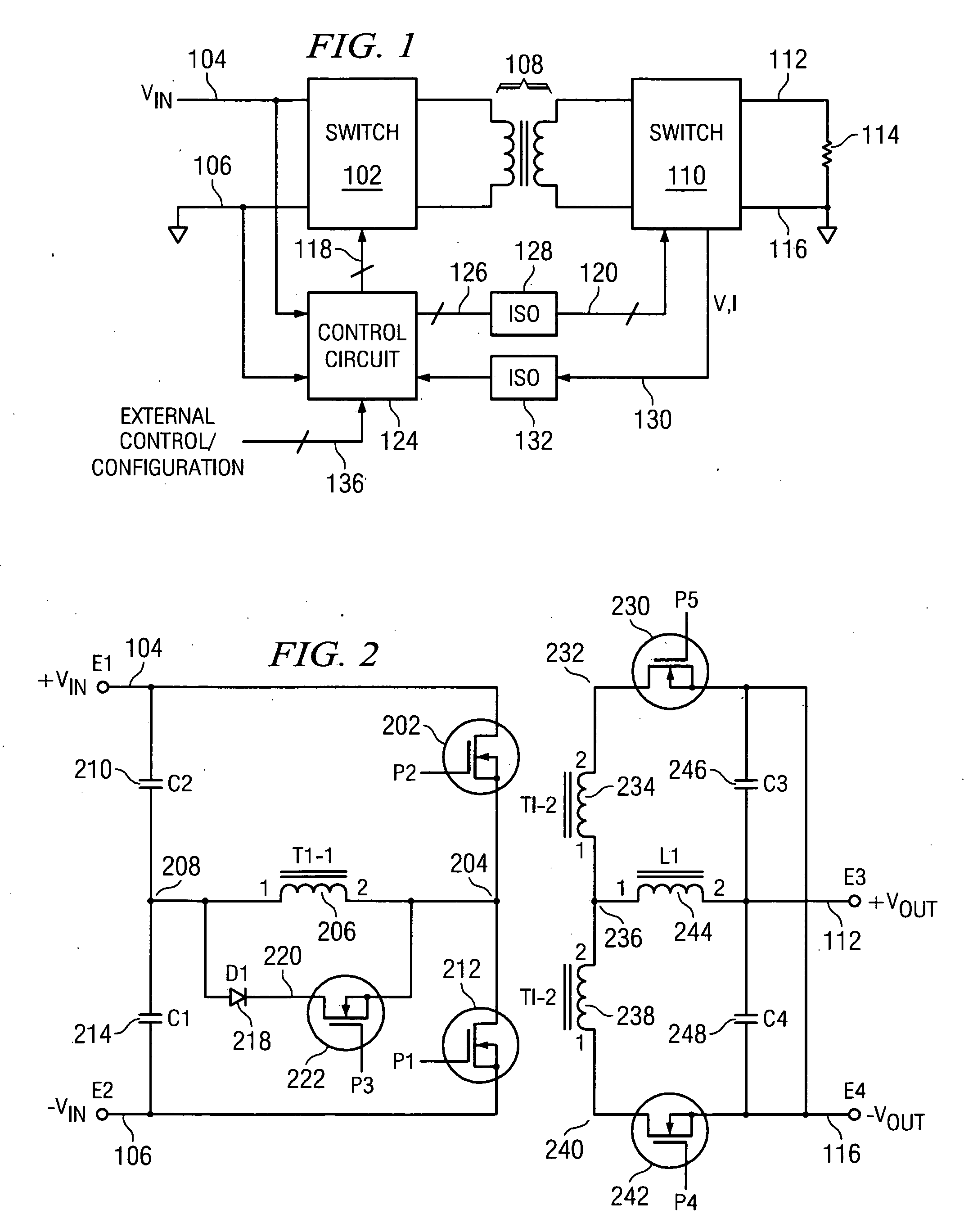
[0047] Referring now to FIG. 1, there is illustrated a top level schematic diagram for the switching power supply of the present embodiment, which in this FIG. is illustrated as a half bridge power supply. The main portion of the power supply comprises a primary switch group 102 that is operable to receive an input voltage on a node 104, this being a DC voltage, and ground on a node 106. The primary switch group 102 is coupled through an isolation transformer 108 to a secondary switch group 110. The secondary switch group 110 is operable to drive an output voltage node 112 that is connected to one terminal of a load 114, the secondary switch group 110 also having a ground connection on a node 116, the load 114 disposed between the node 112 and the node 116. The two switch groups 102 and 110 are operable to operate in conjunction with various pulse inputs on a control bus 118 associated with the primary switch group 102 and with various pulse inputs on a control bus 126 associated wi...


PUM


Abstract

A system for optimizing the power efficiency of a switching power converter operating at a switching frequency includes a digital controller for receiving an analog signal representing an output DC voltage of the switching power converter for comparison to a desired output voltage level and generating switching control signals to control the operation of the power supply to regulate the output DC voltage to said desired output voltage level. At least two of the switching control signals have a dead time between a first edge of a first control signal and a second edge of a second control signal. The dead time is programmable to control a power efficiency of the switching power converter. The switching control signals additionally switch the power supply between a continuous conduction mode and a discontinuous conduction mode responsive to a mode control signal. The operation of the digital controller is parameterized by a set of operating parameters. A driver circuit is connected to an output of the digital controller to drive the switching control signals and further includes an input for a regulated voltage. The voltage regulator selects the regulated voltage to the driver circuit responsive to a voltage control signal. A micro controller determines the parameters used by said digital controller, establishes the programmable dead time between the control signals to substantially maximize power efficiency of the switching power converter, generates a voltage control signal to substantially maximize the power efficiency of the switching power converter and generates the mode control signal responsive to a current signal from the switching power converter. The micro controller operates independently of the operation of the digital controller.

Description

CROSS-REFERENCE TO RELATED APPLICATIONS [0001] This application is related to U.S. patent application Ser. No. 11 / 172,344 filed on Jun. 30, 2005 entitled “DIGITAL PWM CONTROLLER FOR DIGITAL POWER SUPPLY HAVING PROGRAMMABLE DEAD TIMES” (Atty. Dkt. No. CYGL-27,161) and is incorporated herein by reference.TECHNICAL FIELD OF THE INVENTION [0002] The present invention relates to DC-DC power converters, and more particularly, to a point of load digital controller having optimized voltages. BACKGROUND OF THE INVENTION [0003] DC-DC power converters are utilized in situations where one DC voltage is converted to another DC voltage. In one application, that associated with PC based systems, the processor requires a fairly low voltage and a fairly high current. Rather than convert an incoming AC voltage down to a very low DC voltage and then route the low DC voltage across a PC board, a higher DC voltage is output by the power supply, routed around to the various components on the PC board and...

Claims


Application Information

Patent Timeline
Patent Type & Authority Applications(United States)
IPC IPC(8): H02M3/335
CPCH02M7/219H02M2007/2195Y02B70/1408H02M7/2195Y02B70/10
Inventor LEUNG, KA Y.
Owner SILICON LAB INC
Learn More