Design of high-frequency substrate noise isolation in BiCMOS technology

a high-frequency substrate and noise isolation technology, applied in the field of integrated circuit isolation, can solve the problems of noise coupling between digital and analog circuits, noise interference also exists between digital circuit components, and analog circuits are especially affected by the noise generated in digital circuits, and achieve good isolation

Inactive Publication Date: 2007-06-28
TAIWAN SEMICON MFG CO LTD
View PDF15 Cites 18 Cited by
  • Summary
  • Abstract
  • Description
  • Claims
  • Application Information

AI Technical Summary

Benefits of technology

[0013] The preferred embodiments of the present invention provide a good isolation between integrated circuits, particularly for integrated circuits operating at high frequencies.

Problems solved by technology

The integration of the digital and analog circuits causes noise coupling between digital and analog circuits.
Analog circuits are especially affected by the noise generated in digital circuits.
Besides the noise interference between digital circuits and analog circuits, noise interference also exists between digital circuit components.
However, even deep trench isolation is not fully satisfactory when a full isolation between the circuits is required.
However, when the die size of the integrated circuit, which mostly consists of analog and digital blocks, becomes smaller in advanced technologies, and / or the frequency increases to over about 1 GHz, noise interference becomes more severe and better isolation techniques are needed.

Method used


Image

  • Design of high-frequency substrate noise isolation in BiCMOS technology
  • Design of high-frequency substrate noise isolation in BiCMOS technology
  • Design of high-frequency substrate noise isolation in BiCMOS technology

Examples


Embodiment Construction

[0022] The making and using of the presently preferred embodiments are discussed in detail below. It should be appreciated, however, that the present invention provides many applicable inventive concepts that can be embodied in a wide variety of specific contexts. The specific embodiments discussed are merely illustrative of specific ways to make and use the invention, and do not limit the scope of the invention.

[0023] The preferred embodiments are illustrated in FIGS. 4 through 12, wherein like reference numbers are used to designate like elements throughout the various views and illustrative embodiments of the present invention.

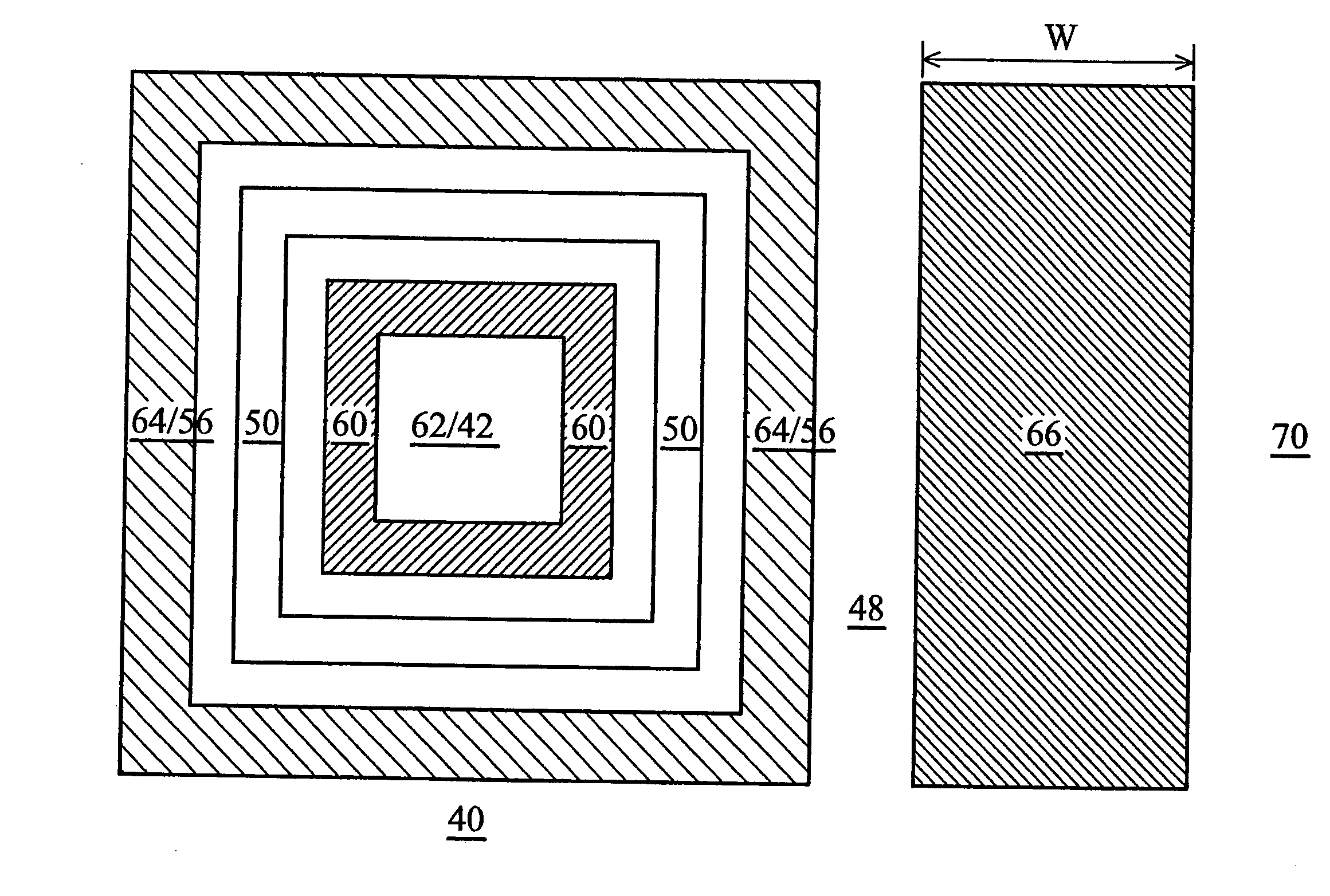
[0024]FIG. 4 illustrates the formation of an N+ buried layer (NBL) 42 in a substrate 40. Substrate 40 preferably comprises a semiconductor material such as silicon, although other semiconductor materials such as Ill-V group related compounds (for example, GaAs and InP) may also be used. In the preferred embodiment, substrate 40 is of p-type. In other embo...


PUM


Abstract

A high-frequency noise isolation structure and a method for forming the same are provided. The noise isolation structure isolates a first device region and a second device region over a semiconductor substrate. The noise isolation structure preferably includes a sinker region substantially encircling a first device region, a buried layer underlying the first device region and joining the sinker region, a deep guard ring substantially encircling the sinker region, and a deep trench oxide region substantially encircling the sinker region. The isolation structure further includes a wide guard ring between the first and the second device regions. The sinker region and the buried region preferably have a high impurity concentration. Integrated circuits to be noise decoupled are preferably formed in the respective first and second device regions.

Description

TECHNICAL FIELD [0001] This invention relates generally to integrated circuit isolation, and particularly relates to noise isolation between integrated circuits operated at high frequencies. BACKGROUND [0002] Recent advances in bipolar / BiCMOS IC design and fabrication make possible the integration of digital and analog circuits on the same IC chip. This technology is widely used in mobile communication systems where a digital core is combined with analog RF circuits. The digital and analog circuits are typically formed as a variety of components near one surface of a wafer. These components may be at several levels separated by inter-metal dielectric layers. Usually, the topmost layer is made of a dielectric material and serves as a passivation layer for the entire structure. [0003] The integration of the digital and analog circuits causes noise coupling between digital and analog circuits. Analog circuits are especially affected by the noise generated in digital circuits. This sign...

Claims


Application Information

Patent Timeline
Patent Type & Authority Applications(United States)
IPC IPC(8): H01L29/76
CPCH01L21/761H01L21/823878
Inventor YEH, DER-CHYANGLEE, CHUAN-YINGYEH, VICTOR P.C.
Owner TAIWAN SEMICON MFG CO LTD
Why Eureka
Try Eureka