
Optical data processing apparatus using vertical-cavity surface-emitting laser (VCSEL) device with large oxide-aperture

a technology of optical data processing and surface-emitting laser, which is applied in the direction of lasers, optical resonator shape and construction, semiconductor lasers, etc., can solve the problems of device deformation, device deformation, and variable diameter

Inactive Publication Date: 2007-06-28
FUJIFILM BUSINESS INNOVATION CORP
View PDF7 Cites 16 Cited by
  • Summary
  • Abstract
  • Description
  • Claims
  • Application Information

AI Technical Summary

Benefits of technology

[0008]When a VCSEL is used as a light source of, for example, an electrophotographic image forming apparatus (scanning exposure apparatus) such as a laser printer, in order to obtain high resolution, it is required that small light-emitting spots be connected on a surface of a photoconductor drum. In other words, because it is required that the radiation light of the VCSEL be focused by a lens, a single-mode (fundamental transverse mode lasing) is preferred whose emission intensity distribution is Gaussian-like. As a result, for applications such as a high-resolution laser printer, a VCSEL in which the diameter of the non-oxidized region is equal to or smaller than nearly 4 micrometers has been used.
[0008]When a VCSEL is used as a light source of, for example, an electrophotographic image forming apparatus (scanning exposure apparatus) such as a laser printer, in order to obtain high resolution, it is required that small light-emitting spots be connected on a surface of a photoconductor drum. In other words, because it is required that the radiation light of the VCSEL be focused by a lens, a single-mode (fundamental transverse mode lasing) is preferred whose emission intensity distribution is Gaussian-like. As a result, for applications such as a high-resolution laser printer, a VCSEL in which the diameter of the non-oxidized region is equal to or smaller than nearly 4 micrometers has been used.
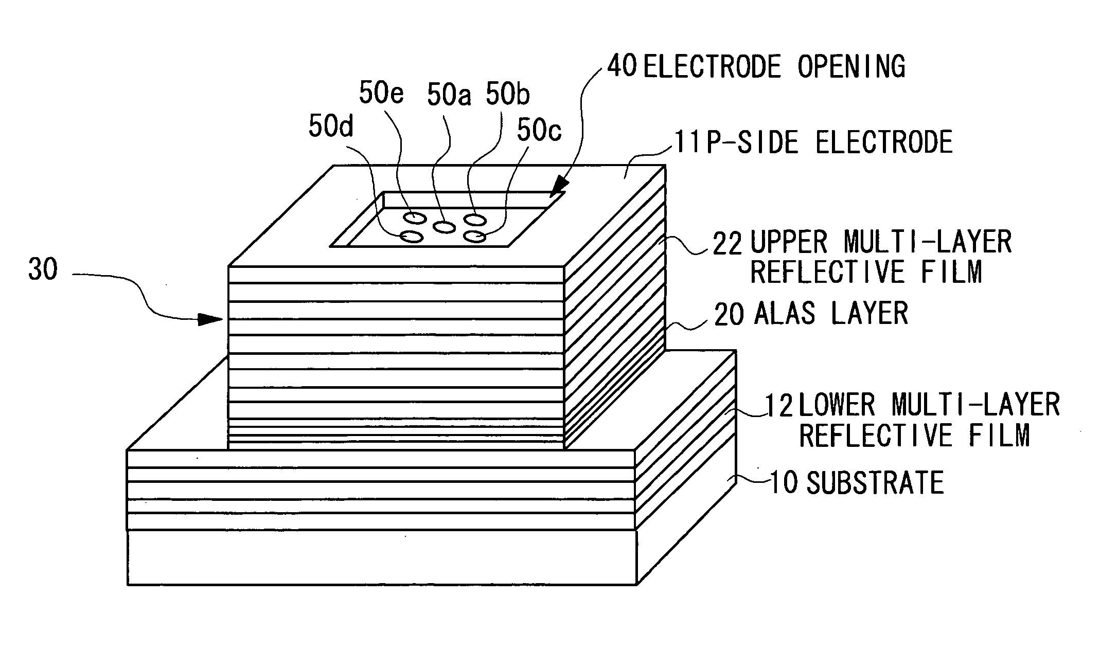
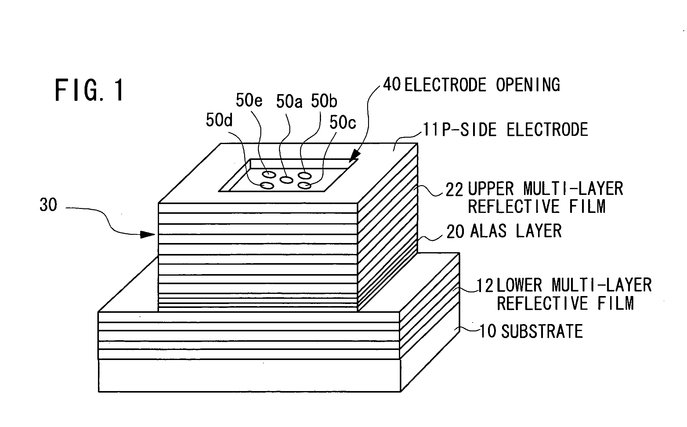
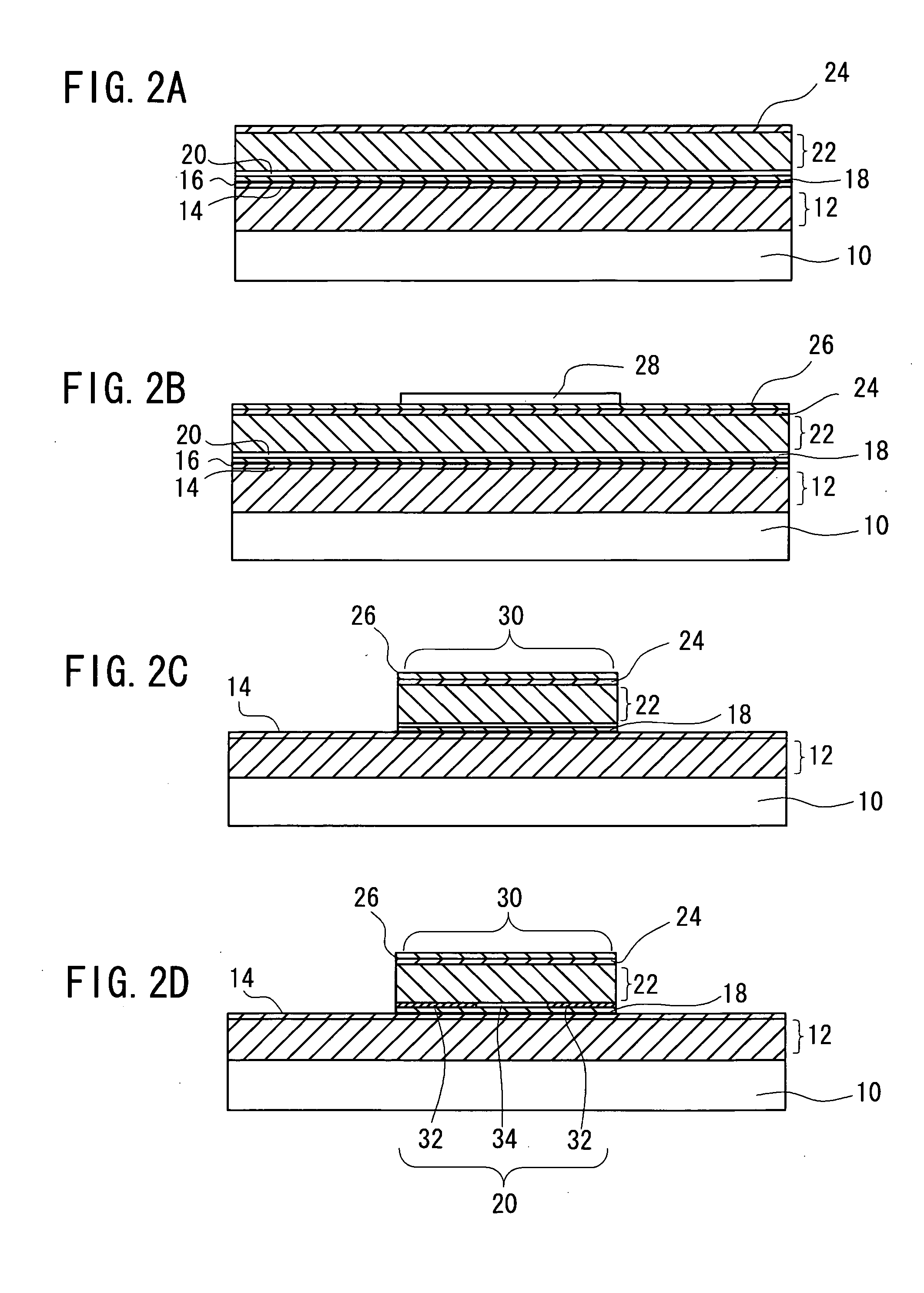
[0012]An aspect of the present invention provides an optical data processing apparatus including a light source, an optical system that concentrates light from the light source to an optical data storage medium, and a mechanism that scans the concentrated laser light on the optical data storage medium. The light source includes at least one Vertical-Cavity Surface-Emitting Laser (VCSEL) device that emits laser light, and the at least one VCSEL device includes an active region and a current-confined portion between first and second mirrors that form a vertical resonator structure. In the current-confined portion, an opening having a diameter larger than about 4 micrometers is formed for current injection.
[0057]FIG. 13C shows the relation between the bias current and light output (shown by circles) and divergence angle (shown by triangles) for a VCSEL that generates a high-order single-mode lasing. For comparison, measurements obtained for a normal multi-mode VCSEL (FIG. 13B), and a single-mode VCSEL (FIG. 13A) are also shown. The diameter of the non-oxidized region of the multi-mode VCSEL is 8 micrometers, same as that of the high-order single-mode VCSEL; and that of the single-mode VCSEL is 3 micrometers.
[0058]As is evident from the measurements, the divergence angle of the high-order single-mode VCSEL is stable over a wide light output range, and its variation is as small as that of the single-mode VCSEL. For example, in FIG. 13C, the divergence angle at the time the light output starts is about 20 degrees. And the divergence angle at the time the light output reaches a peak at about 5 mW is about 21 degrees, and thus its variation is equal to or smaller than about 5%. Rather, as its opening diameter is larger than that of the single-mode VCSEL, absolute value of the divergence angle is smaller than that of the single-mode VCSEL. Therefore, it can be found that, it is possible to connect small light-emitting spots even in a high-order transverse mode lasing, as same as in the case of a fundamental transverse mode lasing.
[0059]As mentioned above, by using a high-order single-mode device, light-emitting spots with small variation can be easily obtained on the surface of a photoconductor drum. Therefore, a VCSEL that improves yield and has smaller variation in characteristics can be easily obtained, and thus a lower-cost scanning exposure apparatus can be obtained.
[0060]From the measurements described above, it also can be found that, even with a multi-mode VCSEL, the variation in divergence angle can be maintained small if the bias current range is limited near threshold. Therefore, even though surface processing is not provided on the substrate, single-peaked pattern emission profile can be obtained by operating the device near threshold current. This denotes the applicability of a multi-mode VCSEL to a scanning exposure apparatus.
[0061]As such, according to an optical data processing apparatus using a VCSEL of an example, by using a high-order single-mode VCSEL or a multi-mode VCSEL, either of whose non-oxidized region has a diameter of larger than 4 micrometers, and more preferably equal to or larger than 8 micrometers, as a light source, an optical data processing apparatus can be obtained in which ESD damage threshold and reliability of the device can be dramatically improved, and device-to-device variation in characteristics due to the variation in diameter of the non-oxidized region is small, all of which will lead to cost reduction.

Problems solved by technology

The control requires complicated fabrication processes, which may cause wafer-to-wafer variation in diameter, and thus reduce yield.
In addition, the smaller the diameter of the non-oxidized region is, the less the ESD damage threshold and reliability become as shown above, and thus the faster the device degrades, which shortens the life.
The life of the device decides the life of a product, and thus the degrading its life requires an additional cost, for example, preparing replacement parts.
Therefore, it has been a cause of high cost to use a small-aperture single-mode VCSEL, whose non-oxidized region has a diameter of equal to or smaller than 4 micrometers typically, as a light source of an image forming apparatus such as a laser printer.

Method used


Image

  • Optical data processing apparatus using vertical-cavity surface-emitting laser (VCSEL) device with large oxide-aperture
  • Optical data processing apparatus using vertical-cavity surface-emitting laser (VCSEL) device with large oxide-aperture
  • Optical data processing apparatus using vertical-cavity surface-emitting laser (VCSEL) device with large oxide-aperture

Examples


Embodiment Construction

[0027]A description will now be given, with reference to the accompanying drawings, of embodiments of the present invention.

[0028]Now examples of a scanning exposure apparatus using a VCSEL according to an aspect of the invention will be described referring to the accompanying drawings.

[0029]FIG. 1 is a perspective view of a VCSEL according to an example of the present invention. The VCSEL in the example includes a rectangular parallelepiped post portion 30 on a substrate 10. In an electrode opening 40 at a top portion of the post portion 30, multiple holes 50a, 50b, 50c, 50d, and 50e are formed. In an AlAs layer 20 in the post portion 30, a non-oxidized region having a diameter of about 8 micrometers is formed. A VCSEL having such a configuration emits a high-order single-mode laser light, as described later.

[0030]FIGS. 2A to 3D are cross sectional views to show a method for manufacturing a VCSEL shown in FIG. 1. First, as shown in FIG. 2A, by Metal Organic Chemical Vapor Depositio...


PUM


Abstract

A optical data processing apparatus included a light source, an optical system that concentrates light from the light source to an optical data storage medium, and a mechanism that scans the concentrated laser light on the optical data storage medium, the light source includes at least one Vertical-Cavity Surface-Emitting Laser (VCSEL) device that emits laser light, the at least one VCSEL device included an active region and a current-confined portion between first and second mirrors that form a vertical resonator structure, and an opening having a diameter equal to or larger than about 4 micrometers is formed in the current-confined portion for applying current.

Description

BACKGROUND[0001]1. Technical Field[0002]The present invention relates to an optical data processing apparatus using a Vertical-Cavity Surface-Emitting Laser (hereinafter referred to as VCSEL) device, and more specifically relates to the use of a large-aperture VCSEL for an image forming apparatus such as a copier or printer.[0003]2. Related Art[0004]A VCSEL device is a type of a laser diode, in which light is emitted from main surface side of a semiconductor substrate. VCSELs have outstanding characteristics over edge-emitting semiconductor laser devices that had been used, such as a lower driving current. Moreover, wafer-level inspection can be conducted, and VCSELs can be easily arranged two-dimensionally. Therefore, VCSELs have been used as light sources in various fields of optical data processing, for example, optical communication, or data storage or image formation by the use of light.[0005]In a VCSEL, a current-confined structure is required to effectively control current in...

Claims


Application Information

Patent Timeline
Patent Type & Authority Applications(United States)
IPC IPC(8): H01S5/00H01S3/08
CPCB82Y20/00H01S5/02284H01S5/02288H01S5/18311H01S5/1835H01S5/18358H01S5/18391H01S5/3432H01S2301/166H01L2224/92244H01L2224/82H01L2224/24H01L2224/73267H01S5/02251H01S5/02253H01S5/183H01L2224/18
Inventor UEKI, NOBUAKI
Owner FUJIFILM BUSINESS INNOVATION CORP
Learn More