Wafer measurement system and apparatus

a measurement system and wafer technology, applied in the direction of measurement devices, semiconductor/solid-state device testing/measurement, instruments, etc., can solve the problems of affecting the quality of wafers, and unable to align masks

Inactive Publication Date: 2007-06-28
MARX DAVID S +3
View PDF8 Cites 94 Cited by
  • Summary
  • Abstract
  • Description
  • Claims
  • Application Information

AI Technical Summary

Benefits of technology

[0036]The angle gage block is then turned to present the angle gage block to the second sensor, repeating steps as applied to the first sensor. Then there is a third stage for measuring the localized thickness of the wafer, the thickness measurement further comprising placement of the wafer in a suitable holder allowing the first and second sensors to receive responses from both sides of the wafer.

Problems solved by technology

The wafer is so warped that the masks can never be aligned because the optical equipment cannot focus on the entire surface at once.
This type of problem is costly to semiconductor manufacturers due to reduced yields.
The limitations and shortcomings of this technique have only recently become significant as the accuracy of the required measurement increases and the wafers have become significantly thinner.
This can be problematic if the wafer has multiple materials or is bumped with solder bumps.
More importantly, however, is that the resolution of the capacitance sensors is no longer fine enough to satisfy the increasingly tight requirements of the manufacturers.
Related to the problem of measurement of the thickness of thin wafers is the problem of measuring trench depth on wafers.
However, current methods of measuring the trench are severely limited.
Manufacturers of MEMS devices do not currently have an accurate and inexpensive method to non-destructively measure the depth of etched high aspect ratio trenches.
Current metrology technology cannot measure the depth of high aspect ratio trenches with speed and accuracy.
In addition, these trenches typically have rounded or rough bottoms that absorb any incident light.
Currently, the only method to measure these trenches involves destructively cutting the wafer.
Because of the very steep sidewalls inherent in such trench structures, profiling instruments that use a stylus or other method of contact cannot accommodate an aspect ratio or lateral dimension of this nature.
For example, atomic force microscopes (AFM) and stylus profilers are not suitable because even if the tip could penetrate the trench, it would not be able to follow the side wall, and the tip would break when exiting the trench.
However, the steep walls of the trench prevent much of the light from reaching the bottom of the trench.
The light that enters these trenches might be completely absorbed.
If there is no light returned, then no method of analysis can possibly determine the depth of the trench.
Aside from these fundamental problems, each of the listed non-contact methods has problems unique to that particular method.
Standard confocal microscopes fail because they confuse the signal from the top of the trench with the signal from the bottom when the trench is too narrow.
Thus, a confusing signal is generated even when the bottom of the trench is far away from the focal plane.
Confocal microscopes are also very slow since they require scanning the measurement sample axially to find the plane of best focus.
White light interferometers have similar difficulties in that they are slow and must scan axially.
In addition, the fringe signal is weak due to the light scattered from the walls and the top.
Phase shift interferometers fail outright because phase unwrapping fails to detect steep sidewalls.
Finally, triangulation techniques can only succeed if precise control of the direction of the incident beam relative to the direction of the trench is maintained so that the light can get into the trench from the side.
This constraint makes such an instrument infeasible.

Method used


Image

  • Wafer measurement system and apparatus
  • Wafer measurement system and apparatus
  • Wafer measurement system and apparatus

Examples


Embodiment Construction

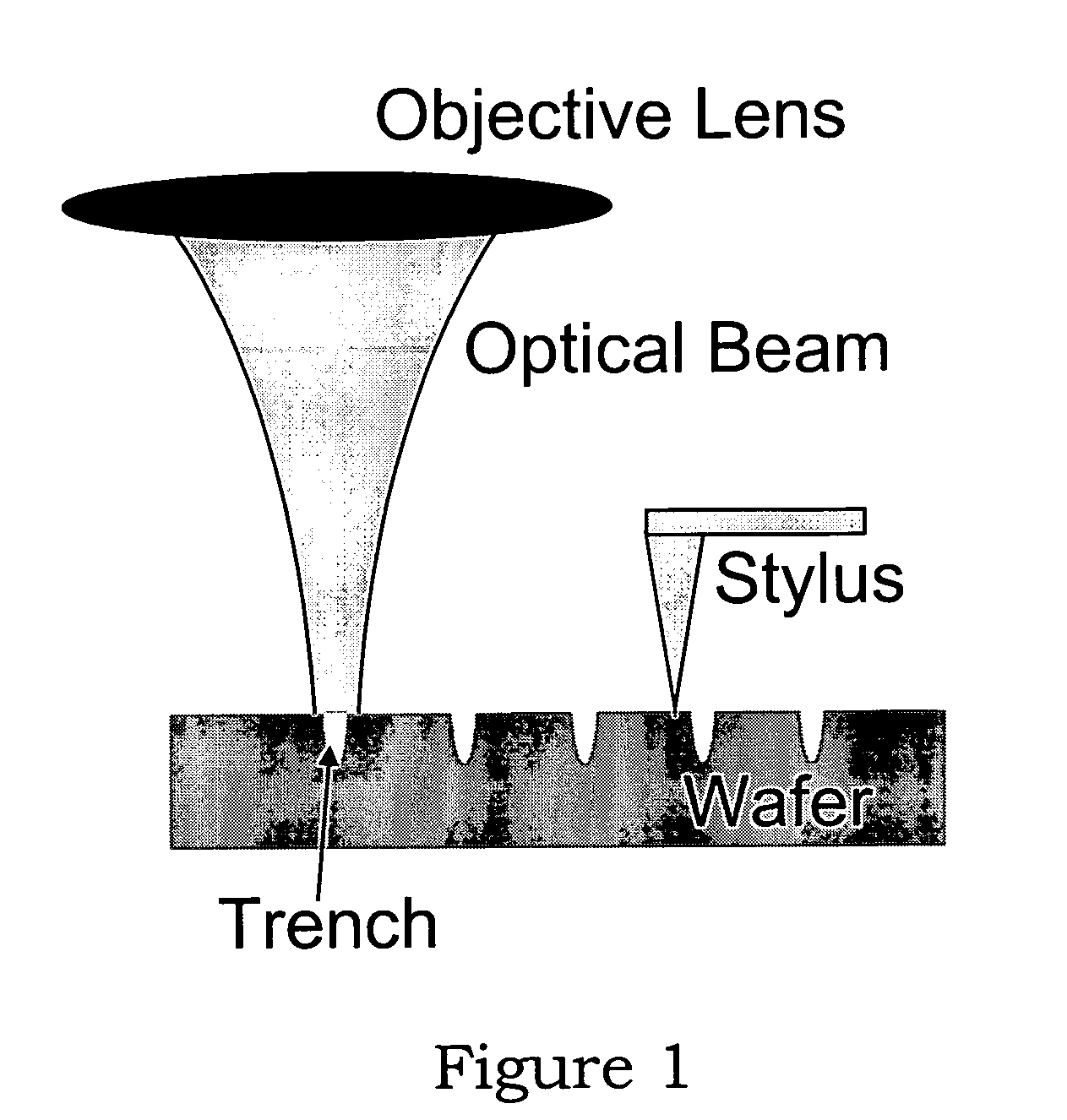
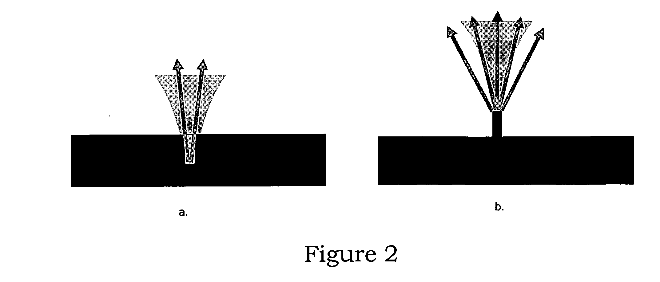
[0054]The instant invention seeks to measure thin wafer thickness as well as the depth of any trench etched thereon. An optical stylus is used that can be thought of as a stylus of light. The stylus has a different color focus at different levels. Thus, any part that reflects the light of the optical stylus will only reflect color that is in focus. FIG. 8 shows the optical stylus. The system then relates color to height. The stylus scans the wafer with whatever density is required by the user, thus acquiring thousands and potentially tens of thousands of data points by which the surface can be defined.

[0055]Regular wafers, i.e., those wafers that have sufficient mass to support their own weight, can be measured by using two optical styli, one from the top and one from the bottom. The separate surfaces acquired by the two styli are related to each other through a calibration operation. Thus, the system can determine the shape and calculate warp, bow, and various other shape values of...


PUM


Abstract

A method and apparatus for the measurement of wafer thickness, flatness and the trench depth of any trenches etched thereon using the back surface of the wafer to accurately measure the back side of a trench, rendering the trench an effective bump, capable of being measured on the top surface and the bottom surface through a non-contact optical instrument that simultaneously measures the wavelength of the top surface and bottom surface of the wafer, converting the distance between wavelengths to a thickness measurement, using a light source that renders the material of which the wafer is composed transparent in that wavelength range, i.e., using the near infrared region for measuring the thickness and trench depth measurement of wafers made of silicon, which is opaque in the visible region and transparent in the near infrared region. Thickness and flatness, as well as localized shape, can also be measured using a calibration method that utilizes a pair of optical styli.

Description

REFERENCE TO PRIOR APPLICATION[0001]This application claims the priority of provisional application 60 / 721,554, filed Sep. 29, 2005 entitled WAFER THICKNESS AND FLATNESS MEASUREMENT SYSTEM by David L. Grant, David S. Marx, Michael A. Mahoney and Tsan Yuen Chen, and provisional application 60 / 787,639, filed Mar. 31, 2006 entitled IMPROVED WAFER TRENCH DEPTH MEASUREMENT SYSTEM by David S. Marx and David L. Grant and provisional application 60 / 754,018, filed Dec. 27, 2005 entitled WAFER THICKNESS AND FLATNESS MEASUREMENT SYSTEM by David S. Marx, David L. Grant, Michael A. Mahoney, and Tsan Yuen Chen.BACKGROUND OF THE INVENTION [0002]1. Field of the Invention[0003]The present invention relates generally to the field of the measurement of silicon wafers used in the production of semiconductors, and particularly to the measurement of the thickness of thin wafers, the flatness and localized shape of thin wafers and the depth of trenches etched thereon.[0004]2. Description of the Prior Art[...

Claims


Application Information

Patent Timeline
Patent Type & Authority Applications(United States)
IPC IPC(8): H01L21/66
CPCH01L22/12
Inventor MARX, DAVID S.GRANT, DAVID L.MAHONEY, MICHAEL A.CHEN, TSAN YUEN
Owner MARX DAVID S
Why Eureka
Try Eureka