

Semiconductor Process Evaluation Methods Including Variable Ion Implanting Conditions
a technology of ion implanting and process evaluation, applied in the direction of individual semiconductor device testing, semiconductor/solid-state device testing/measurement, instruments, etc., can solve the problems of reducing the number of test wafers that pass through a series of processes including an ion implanting process, the inability to reuse test wafers, and the increase in the manufacturing cost of a corresponding semiconductor chip. , to achieve the effect of reducing or minimizing the parameter estimation cost and shortened
- Summary
- Abstract
- Description
- Claims
- Application Information
AI Technical Summary
Benefits of technology
Problems solved by technology
Method used
Image

Examples
Embodiment Construction
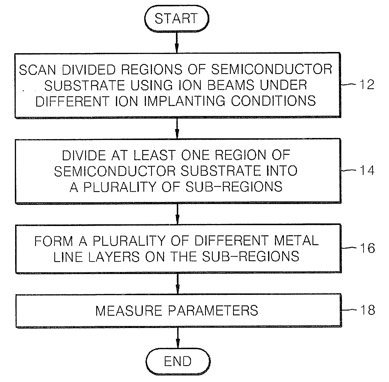
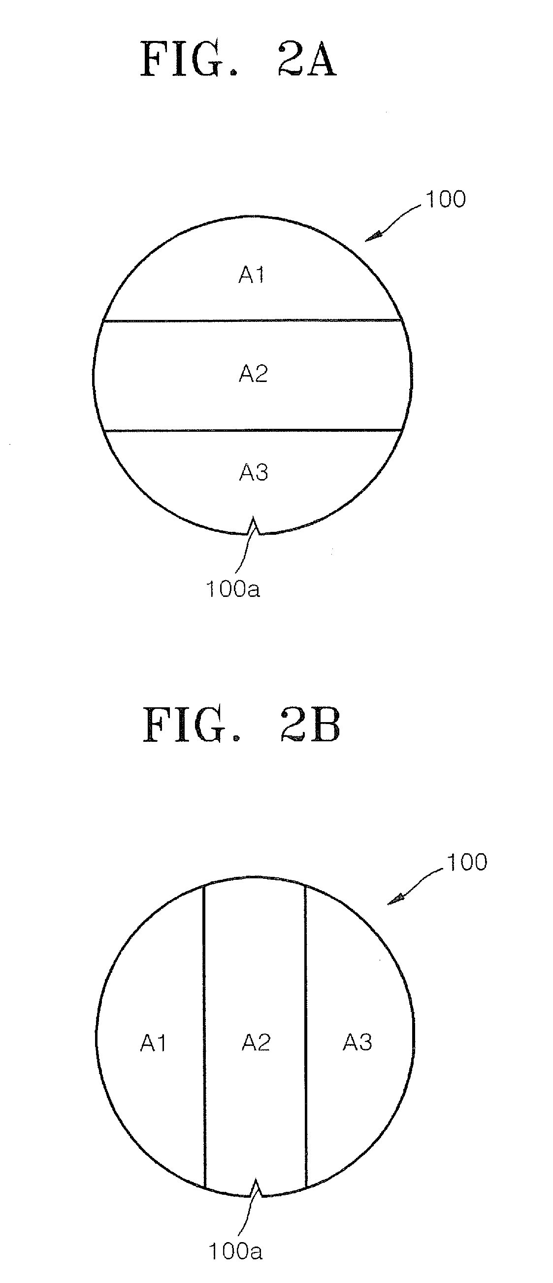
[0032]The invention will be described more fully hereinafter with reference to the accompanying drawings, in which example embodiments of the invention are shown. This invention may, however, be embodied in many different forms and should not be construed as limited to the example embodiments set forth herein. Rather, the disclosed embodiments are provided so that this disclosure will be thorough and complete, and will fully convey the scope of the invention to those skilled in the art. In the drawings, the size and relative sizes of layers and regions may be exaggerated for clarity. Like numbers refer to like elements throughout.
[0033]It will be understood that when an element or layer is referred to as being “on”, “connected to” and / or “coupled to” another element or layer, it can be directly on, connected or coupled to the other element or layer or intervening elements or layers may be present. In contrast, when an element is referred to as being “directly on,”“directly connected...
PUM
 Abstract
Description
Claims
Application Information