Power device utilizing chemical mechanical planarization

a power device and chemical mechanical technology, applied in the direction of semiconductor devices, basic electric elements, electrical equipment, etc., can solve the problems of complex process steps, high cost, and high cost of trench-gated mosfet fabrication processes

Inactive Publication Date: 2007-07-05
SEMICON COMPONENTS IND LLC
View PDF13 Cites 144 Cited by
  • Summary
  • Abstract
  • Description
  • Claims
  • Application Information

AI Technical Summary

Problems solved by technology

Current fabrication processes used to fabricate trench-gated MOSFETs have proven challenging for the semiconductor industry.
Generally, the more complex the device, the more complex the process steps.
The more complex the process steps the more likely a process error will occur.
Using multiple masks to etch adjacent trenches of varying dimensions has proven to be difficult due to errors introduced by the mask dimensions and / or alignment thereof at each masking step.
A single mask misalignment can potentially ruin an entire array of MOSFETs.
Variations in the topography of the substrate surface make it difficult to uniformly deposit onto or etch material from the wafer surface.
For example, variations in topography. make it difficult to bring the entire surface of the substrate in the depth of field of photolithography system, or selectively remove material based on position.

Method used


Image

  • Power device utilizing chemical mechanical planarization
  • Power device utilizing chemical mechanical planarization
  • Power device utilizing chemical mechanical planarization

Examples


Embodiment Construction

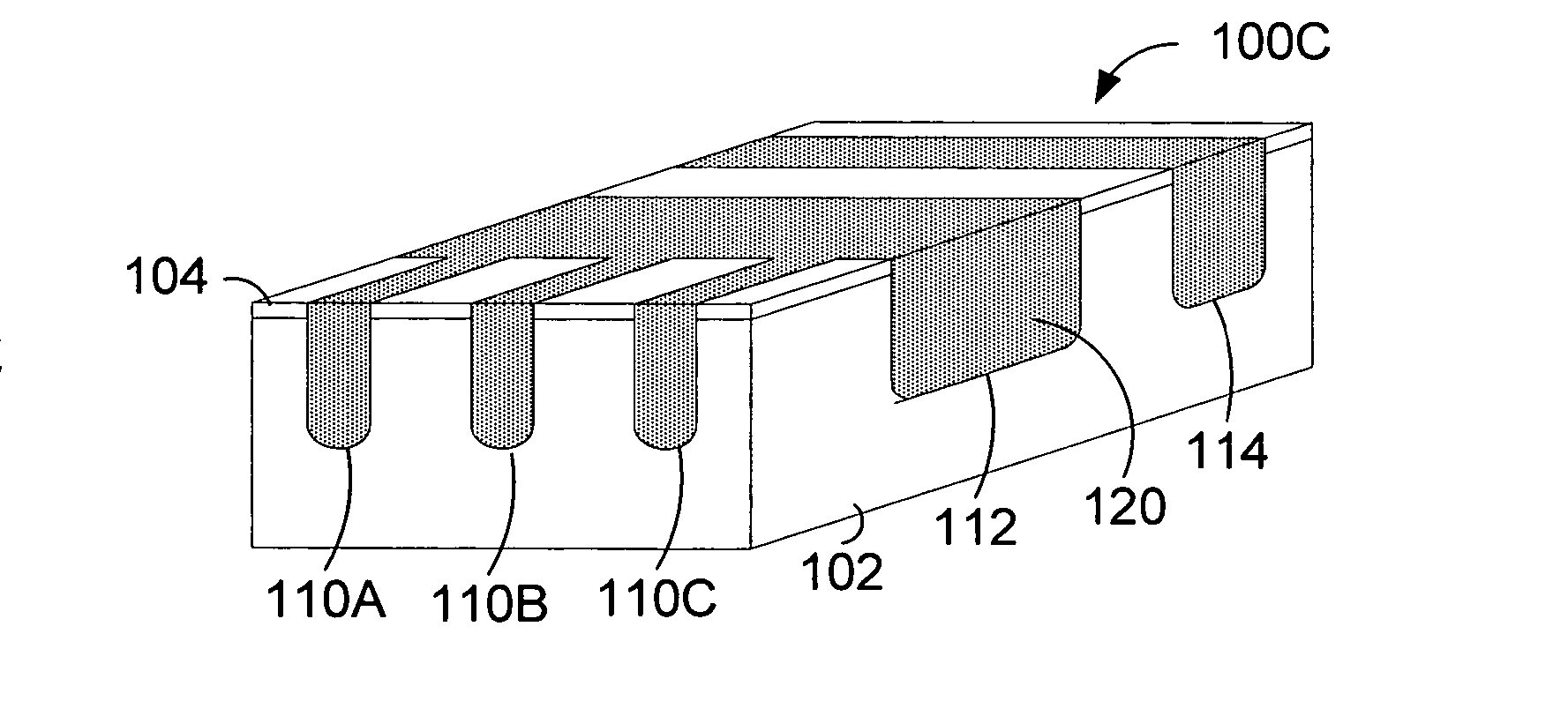
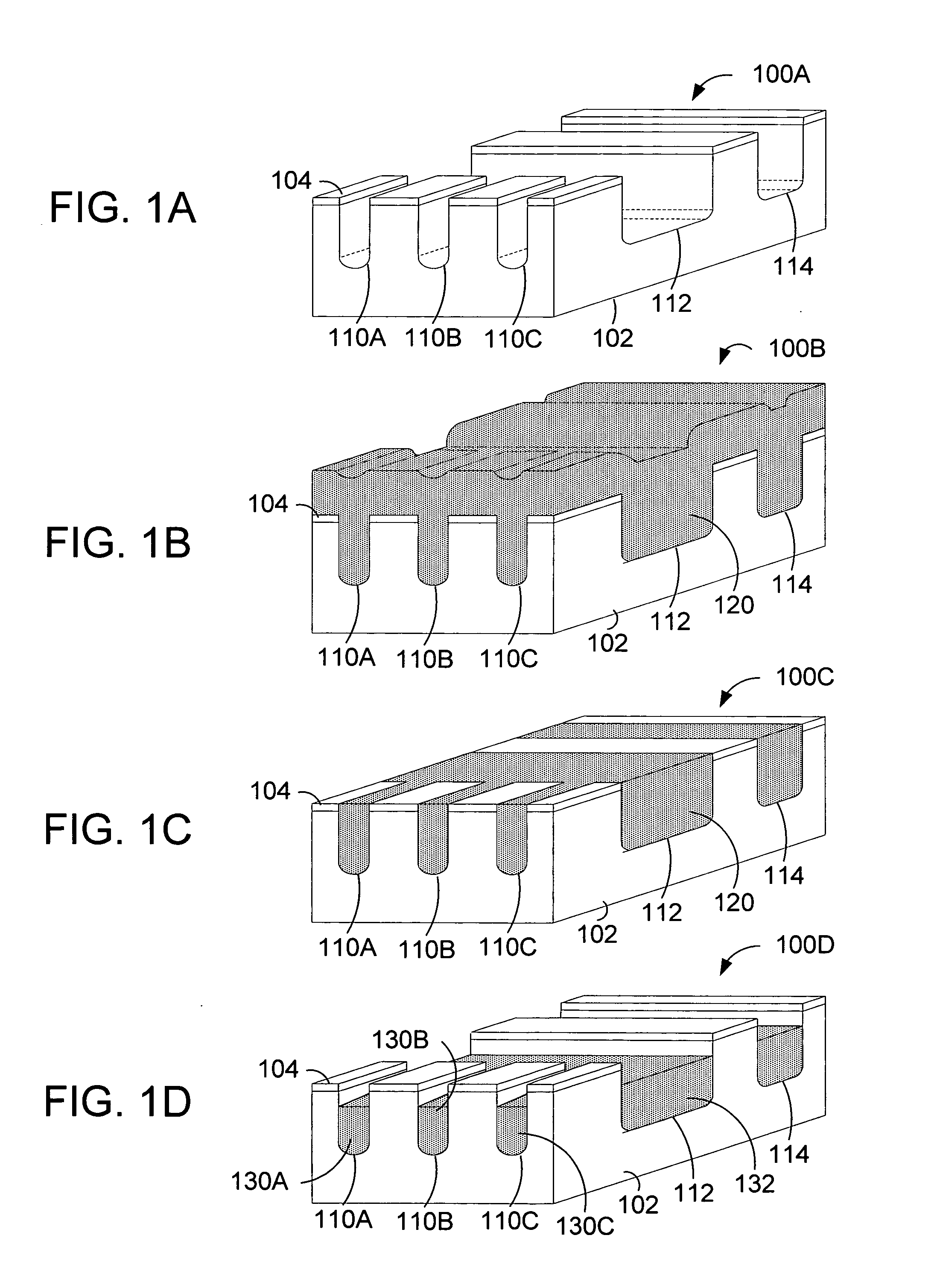
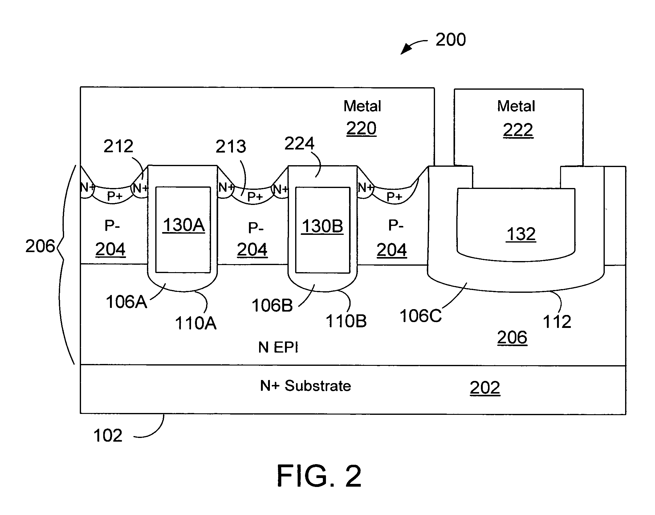
[0029] The present invention pertains to improved trench-gated power device structures and processes used to form the same. In one embodiment, fabrication of the trench-gated vertical power MOSFETs includes forming active gate trenches in the active region and gate runner trenches using a single masking / etching process, wherein the gate runner trenches are wider than the active gate trenches. The single masking / etching process includes forming a mask, such as an oxide, nitride, and the like, on the surface of a substrate. The mask includes apertures corresponding to an array of trenches and other structures. Some of the trenches are active gate trenches that are used to form gate structures associated with power MOSFETs. Other trenches are gate runner trenches used to form interconnect structures which electrically connect a plurality of adjacent gate structures or other structures together. Yet other trenches are termination trenches which typically surround the active region, and ...


PUM


Abstract

A trench-gated field effect transistor (FET) is formed as follows. Using one mask, a plurality of active gate trenches and at least one gate runner trench are defined and simultaneously formed in a silicon region such that (i) the at least one gate runner trench has a width greater than a width of each of the plurality of active gate trenches, and (ii) the plurality of active gate trenches are contiguous with the at least one gate runner trench.

Description

CROSS-REFERENCE TO RELATED APPLICATIONS [0001] This application is related to the commonly assigned U.S. application Ser. No. 11 / 026,276, filed Dec. 29, 2004 which disclosure is incorporated herein by reference in its entirety for all purposes.BACKGROUND OF THE INVENTION [0002] The present invention relates to semiconductor power device technology and more particularly to improved trench-gated power devices and manufacturing processes for forming the same. [0003] Power MOSFETs (metal oxide semiconductor field effect transistors) are well known in the semiconductor industry. One variety of power MOSFETs is the vertically-conducting “trench MOSFET” (e.g., trench DMOS, trench FET, UMOS, etc.). Generally, the trench MOSFET includes vertical trenches formed in a semiconducting layer. The semiconducting layer is disposed on a substrate (i.e., wafer) that forms the trench MOSFET drain. Each trench includes a polysilicon gate insulated from the sidewalls of the trench by a dielectric, gener...

Claims


Application Information

Patent Timeline
Patent Type & Authority Applications(United States)
IPC IPC(8): H01L21/336H01L21/3205
CPCH01L21/3083H01L29/0696H01L29/407H01L29/42368Y10S438/942H01L29/7811H01L29/7813Y10S438/95H01L29/4238
Inventor MARCHANT, BRUCE DOUGLASGREBS, THOMAS E.RIDLEY, RODNEY S.KRAFT, NATHAN LAWRENCE
Owner SEMICON COMPONENTS IND LLC
Why Eureka
Try Eureka