

Circuit substrate and method for fabricating the same
a technology of circuit substrate and substrate, which is applied in the direction of printed circuit manufacturing, printed circuit aspects, printed element electric connection formation, etc., can solve the problems of dielectric breakdown, electrical components often come off, leak current, etc., and achieve the effect of reducing the stress generated in the core substrate, increasing the surface roughness of the inside walls, and reducing the stress of the core substra
- Summary
- Abstract
- Description
- Claims
- Application Information
AI Technical Summary
Benefits of technology
Problems solved by technology
Method used
Image

Examples
first embodiment
A FIRST EMBODIMENT
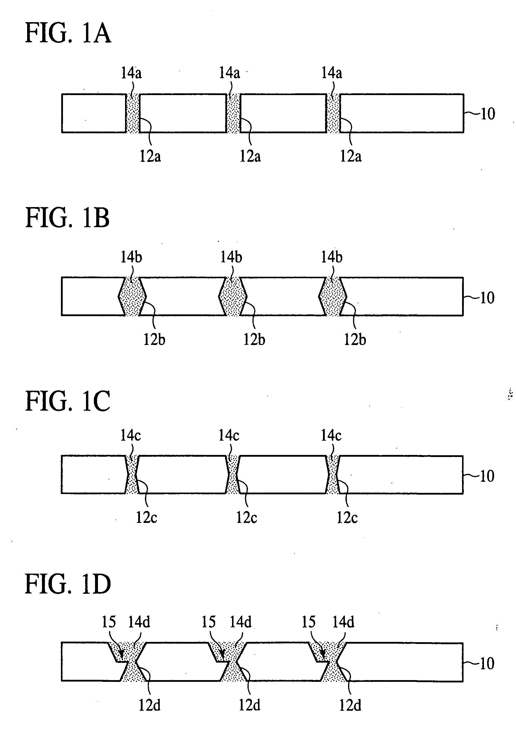
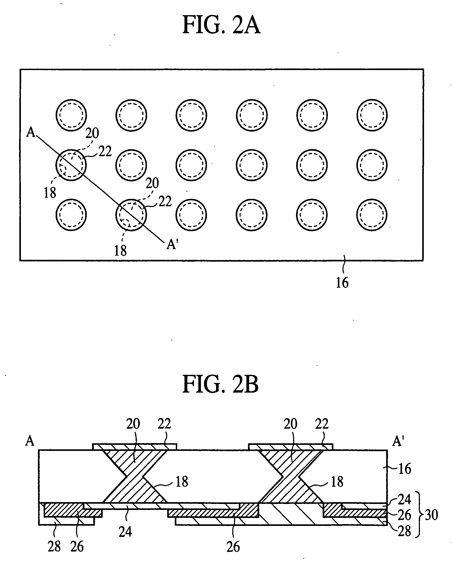
[0037] The circuit substrate according to a first embodiment of the present invention will be explained with reference to FIGS. 2A, 2B, 3A, 3B, 3C, 3D, 4A, 4B, and 4C. FIGS. 2A and 2B are diagrammatic views of the circuit substrate according to the present embodiment, which show a structure thereof. FIGS. 3A, 3B, 3C, 3D, 4A, 4B, and 4C are sectional views of the circuit substrate according to the present embodiment in the steps of the method for fabricating the circuit substrate, which show the method.
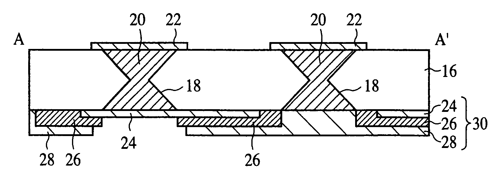
[0038] First, the structure of the circuit substrate according to the present embodiment will be explained with reference to FIGS. 2A and 2B. FIG. 2A is a top view of the circuit substrate according to the present embodiment. FIG. 2B is a sectional view along the line A-A′ in FIG. 2A.
[0039] As shown in FIGS. 2A and 2B, through-holes 18 are formed in a 500 μm-thickness glass substrate 16 at a prescribed pitch. A shape of the through-holes 18 as viewed perpendicularly...
second embodiment
A SECOND EMBODIMENT
[0068] The circuit substrate according to a second embodiment of the present invention will be explained with reference to FIG. 5. FIG. 5 is a sectional view of the circuit substrate according to the present embodiment. The same members of the present embodiment as those of the circuit substrate according to the first embodiment and the method for fabricating the circuit substrate are represented by the same reference numbers not to repeat or to simplify their explanation.
[0069] As shown in FIG. 5, the circuit substrate according to the present embodiment uses a silicon substrate 36 in place of the glass substrate 10 of the circuit substrate according to the first embodiment.
[0070] An insulation film of a 1 μm-thickness silicon oxide film is formed on both surfaces of the silicon substrate 36 and on the inside walls of through-holes 18.
[0071] In the circuit substrate according to the present embodiment, the insulation between the conducting silicon substrate 36...
third embodiment
A THIRD EMBODIMENT
[0082] The circuit substrate according to a third embodiment of the present invention and the method for fabricating the circuit substrate will be explained with reference to FIGS. 6, 7A, 7B, and 7C. FIG. 6 is a sectional view of the circuit substrate according to the present embodiment, which shows a structure thereof. FIGS. 7A, 7B, and 7C are sectional views of the circuit substrate according to the present embodiment in the steps of the method for fabricating the same, which show the method. The same members of the present embodiment as those of the circuit substrate according to the first embodiment and the method for fabricating the semiconductor substrate are represented by the same reference numbers not to repeat or to simplify their explanation.
[0083] First, the circuit substrate according to the present embodiment will be explained with reference to FIG. 6.
[0084] As shown in FIG. 6, in the same way as in the first embodiment, through-holes 40 whose openi...
PUM
| Property | Measurement | Unit |
|---|---|---|
| thickness | aaaaa | aaaaa |
| width | aaaaa | aaaaa |
| thickness | aaaaa | aaaaa |
Abstract
Description
Claims
Application Information