

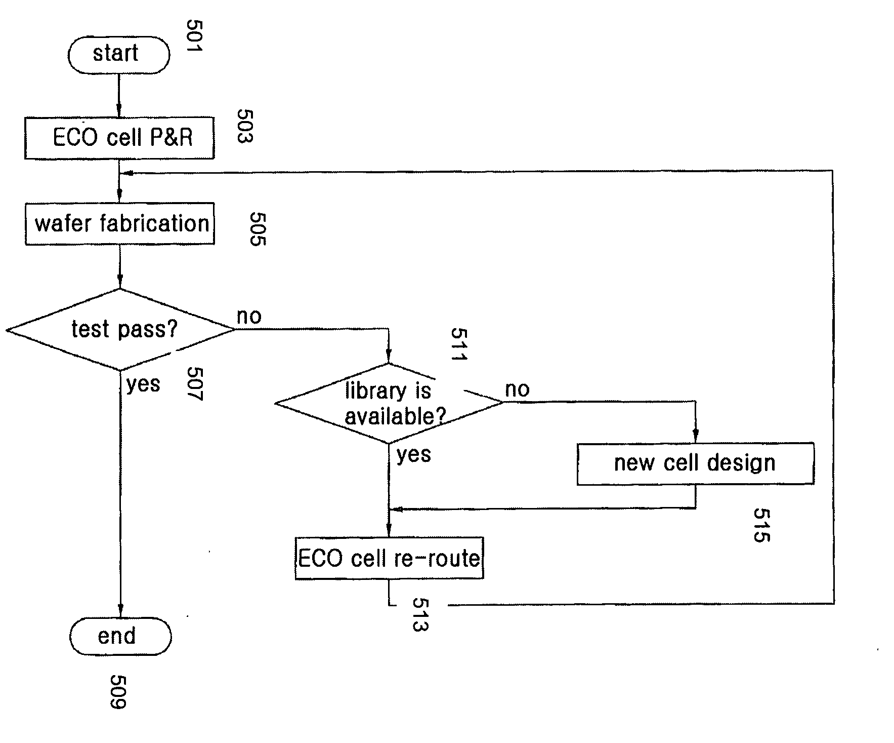
Engineering change order cell and method for arranging and routing the same
a cell and change order technology, applied in the field of engineering change order cell and a method for arranging and routing the same, can solve the problems of poor performance of the cell library used in the eco cell in accordance with the related art, limited flexibility, and problems such as junction capacitance reduction, to achieve the effect of flexibility
- Summary
- Abstract
- Description
- Claims
- Application Information
AI Technical Summary
Benefits of technology
Problems solved by technology
Method used
Image

Examples
first embodiment
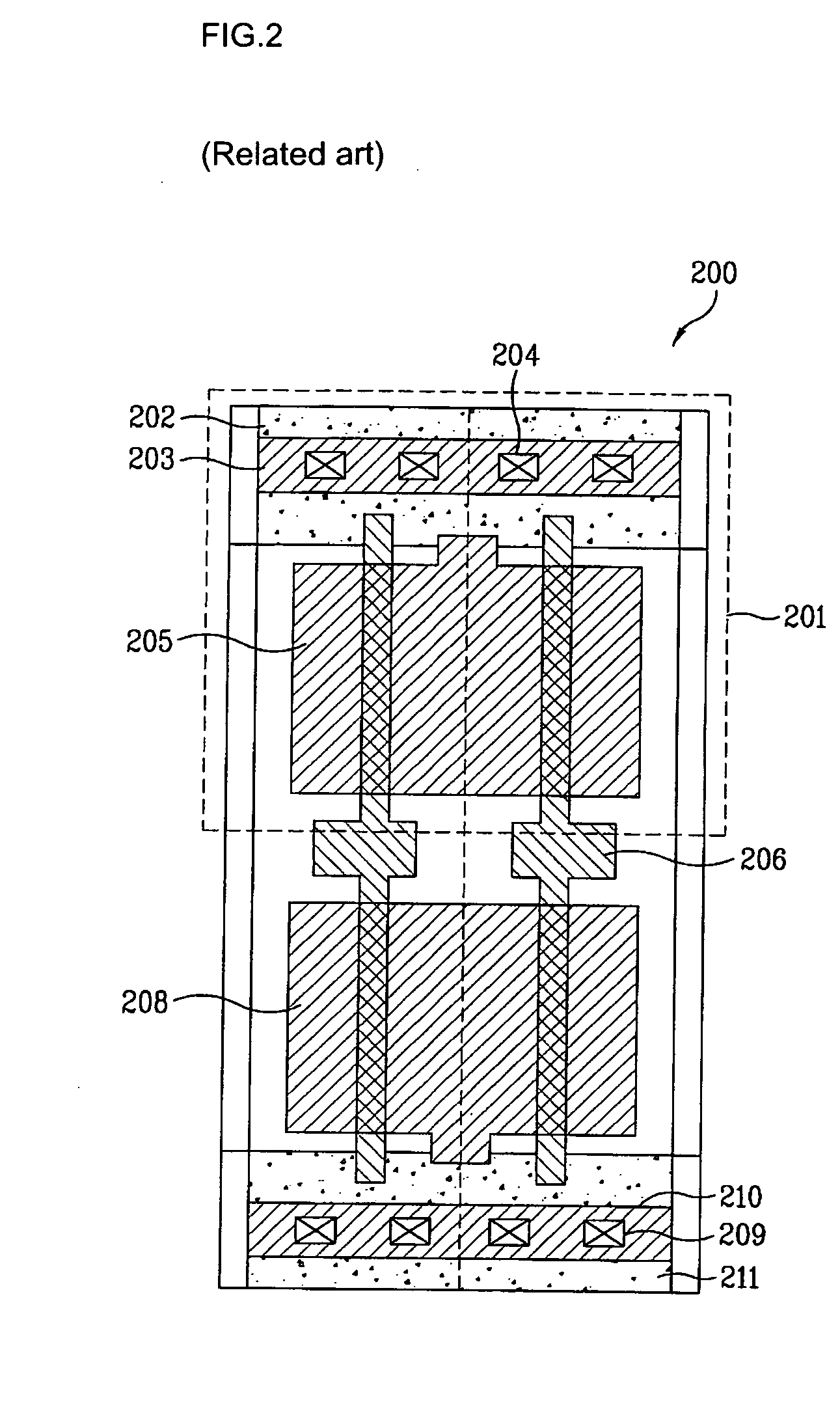
[0038] ECO cell 100 in accordance with a first embodiment consistent with the present invention having the same height with a standard cell, as shown in FIG. 3, includes a VDD power layer 102, an N-diffusion layer 103 for pick up, and a first contact hole 104. VDD power layer 102 may be formed of a metal material, and may be formed in an N-well 101 and provides VDD power. First contact hole 104 connects VDD power layer 102 with N-diffusion layer 103. A P-diffusion layer 105 and a first poly gate 106 for fabricating a PMOS to configure various circuits are further included in ECO cell 100.
[0039] The lower side of ECO cell 100 includes a VSS power layer 111, which may be formed of a metal material, and provides VSS power. The lower side of ECO cell 100 further includes a P-diffusion layer 110 for pick up, and a second contact hole 109 which connects VSS power layer 111 and P-diffusion layer 110. An N-diffusion layer 108 and a second poly gate 107 for fabricating an NMOS to configure v...
second embodiment
[0050] In another embodiment, the diffusion layer for pick-up may be removed in FIG. 3. ECO cell 300 in accordance with a second embodiment consistent with the present invention, as shown in FIG. 4, includes a VDD power layer 302 and a PMOS transistor in N-well 301. VDD power layer 302 is formed on an upper end of ECO cell 300 by a metal material, and provides the VDD power.
[0051] The PMOS transistor includes first poly gate 306 and source and drain regions formed by P-diffusion layer 305.
[0052] A contact hole connecting the VDD power layer with the N-diffusion layer is not formed by not forming the N-diffusion layer for pick-up.
[0053] A lower side of the ECO cell includes a VSS power layer 311 and an NMOS transistor. VSS power layer 311 is formed on a lower end of the ECO cell by a metal material and provides the VSS power.
[0054] The NMOS transistor includes a second poly gate 307 and source and drain regions formed by N-diffusion layer 308.
[0055] The P-diffusion layer for pick...
PUM
 Abstract
Description
Claims
Application Information