Junction structure of organic semiconductor device, organic thin film transistor and fabricating method thereof

Inactive Publication Date: 2007-07-12
CHUNGHWA PICTURE TUBES LTD
View PDF11 Cites 9 Cited by
  • Summary
  • Abstract
  • Description
  • Claims
  • Application Information

AI Technical Summary

Benefits of technology

[0008] Accordingly, the present invention is directed to a junction structure of an organic semi

Problems solved by technology

However, the organic semiconductor doped with impurities has poor stability.
However, this method causes the reduction of the on-off ratio of the organic thin film trans

Method used


Image

  • Junction structure of organic semiconductor device, organic thin film transistor and fabricating method thereof
  • Junction structure of organic semiconductor device, organic thin film transistor and fabricating method thereof

Examples


Embodiment Construction

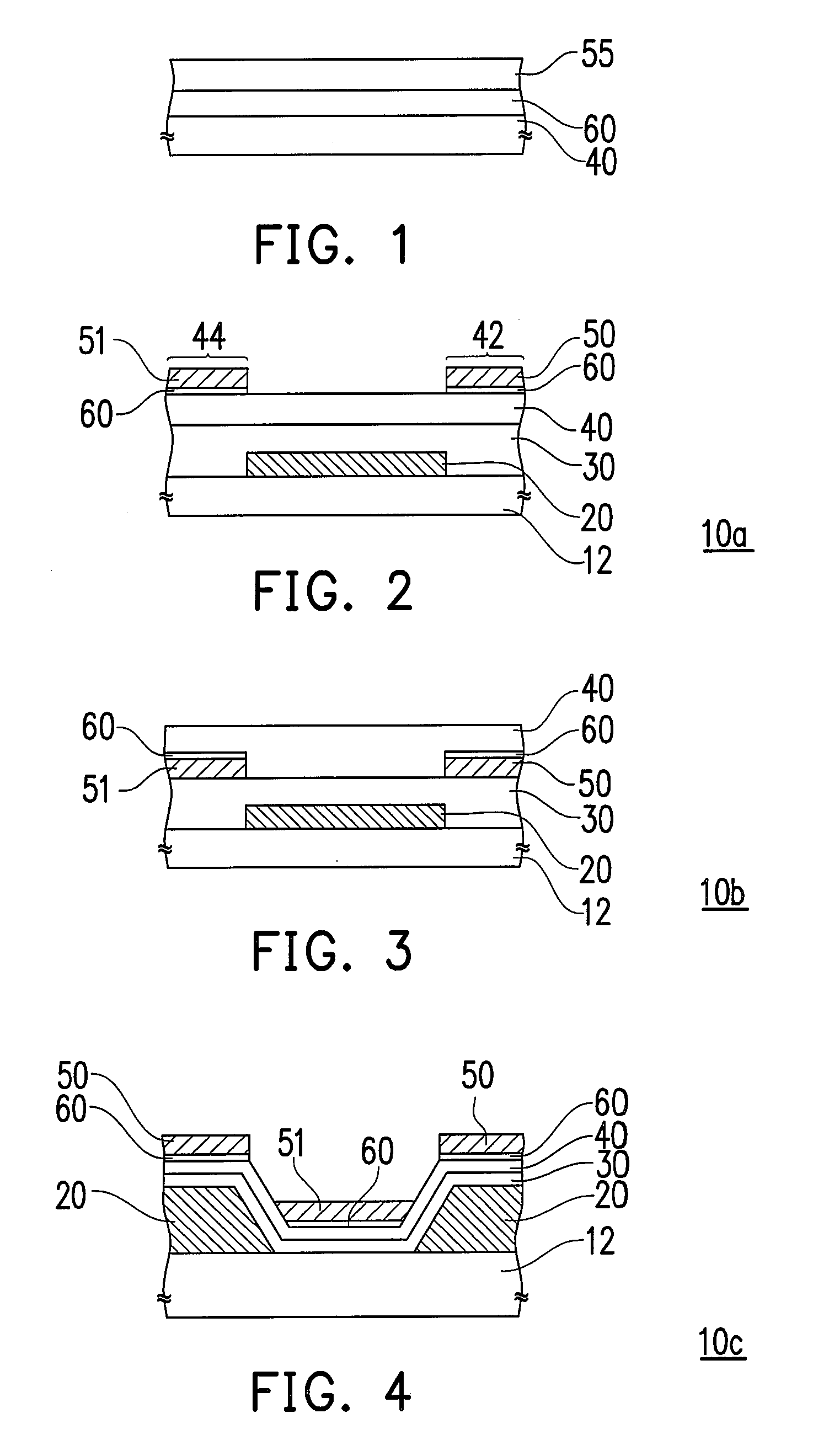
[0030] Reference will now be made in detail to the present preferred embodiments of the invention, examples of which are illustrated in the accompanying drawings. Wherever possible, the same reference numbers are used in the drawings and the description to refer to the same or like parts.

Junction Structure of an Organic Semiconductor Device

[0031]FIG. 1 is a cross-section view showing a junction structure of an organic semiconductor device according to an embodiment of the present invention. As shown in FIG. 1, the junction structure of an organic semiconductor device includes an organic semiconductor layer 40, a conductive layer 55 and a modifying layer 60. The organic semiconductor device is, for example, a metal-oxide-semiconductor (MOS) device, a metal-insulator-semiconductor (MIS) device, a thin film transistor (TFT) or an organic thin film transistor (OTFT). In an embodiment, the material for the organic semiconductor layer 40 comprises a small molecule organic semiconductor...


PUM


Abstract

A junction structure of an organic semiconductor device including an organic semiconductor layer, a conductive layer and a modifying layer is provided. The modifying layer is formed between the organic semiconductor layer and the conductive layer, wherein the modifying layer includes an inorganic compound or an organic complex compound. An organic thin film transistor including a gate, a source/drain, a dielectric layer, an organic semiconductor layer and at least a modifying layer is also provided. The gate is electrically isolated from the source/drain. The dielectric layer is disposed between the gate and the source/drain. The organic semiconductor layer is disposed between the source and the drain. The modifying layer is disposed between the organic semiconductor layer and the source/drain, wherein the modifying layer includes an inorganic compound or an organic complex compound.

Description

CROSS-REFERENCE TO RELATED APPLICATION [0001] This is a continuation-in-part application of patent application Ser. No. 11 / 164,092, filed on Nov. 10, 2005. The entirety of each of the above-mentioned patent applications is hereby incorporated by reference herein and made a part of this specification.BACKGROUND OF THE INVENTION [0002] 1. Field of the Invention [0003] The present invention generally relates to a semiconductor device and a fabricating method thereof. More particularly, the present invention relates to an organic thin film transistor and a fabricating method thereof. [0004] 2. Description of Related Art [0005] Because the organic semiconductor device can be formed on a flexible plastic substrate or a metal substrate, it has advantages of light weight, low cost and flexibility. Thus, organic thin film transistors have been in valued in recent years. [0006] In fabricating methods of the organic thin film transistor, the material for the source / drain is usually metal, such...

Claims


Application Information

Patent Timeline
IPC IPC(8): H01L29/08H01L35/24H01L51/00
CPCH01L51/105H01L51/057H10K10/491H10K10/84
Inventor CHEN, FANG-CHUNGCHUANG, CHIAO-SHUNCHEN, DONG-SIANKUNG, LI-JENLIN, YUNG-SHENGWU, CHUAN-YI
Owner CHUNGHWA PICTURE TUBES LTD
Why Eureka
Try Eureka