
Monolithic mems-based wavelength-selective switches and cross connects

a technology of wavelength-selective switches and monolithic mems, applied in the field of optical switches, can solve the problems of large footprint, high cost of implementation, and high cost of precise alignment, and achieve the effect of reducing insertion loss and crosstalk

Inactive Publication Date: 2007-07-12
RGT UNIV OF CALIFORNIA
View PDF3 Cites 82 Cited by
  • Summary
  • Abstract
  • Description
  • Claims
  • Application Information

AI Technical Summary

Benefits of technology

The present invention provides a way to integrate wavelength-selective switches (WSSs) and wavelength-selective cross connects (WXCs) on a single chip using a one-step etching process. The WSSs and WXCs can be monolithically fabricated on a silicon-on-insulator (SOI) substrate or similar optical substrate materials. The WSSs and WXCs can be used in combination to create optical system elements such as wavelength division multiplexing (WDM) demultiplexers, cross connects, and other optical devices. The WSSs have fast switching times and can be used in the infrared, near-infrared, and visible portions of the electromagnetic spectrum. The WSSs and WXCs are compatible with standard fabrication processes and can be fabricated on SOI or PLC materials. The invention provides a way to integrate WSSs and WXCs on a single chip, which can reduce the size and cost of optical systems.

Problems solved by technology

However, these implementations are costly, require precise alignment, have large footprints, and suffer from additional shortcomings.

Method used


Image

  • Monolithic mems-based wavelength-selective switches and cross connects
  • Monolithic mems-based wavelength-selective switches and cross connects
  • Monolithic mems-based wavelength-selective switches and cross connects

Examples


embodiment 200

[0292]FIG. 65-66 illustrate embodiments of rotary comb-drives having uni-directional and bi-directional deflection. An embodiment 200 of unidirectional deflection mirror is shown in FIG. 65 and provides angular mirror deflection by utilizing a rotary comb-drive actuator. The comb fingers are arranged in concentric arcs to ensure a constant finger gap for the curved contour of rotation. The uni-directional mirror 200 is configured with a base 202 and anchor 204 from which extends a moving element 206 having a mirror surface 208 and comb fingers 210, which being attached to moving element 206 are often referred to as moving comb fingers. Moving element 206 is shown attached to anchor 204 through a compliant spring element 212. Stationary comb fingers 214 extend from base 202 toward interposition between moving comb fingers 210. Displacement of the mirror from initial position 216 is in response to the application of an actuating voltage between the anchor and base, and thus between th...

embodiment 230

[0294]FIG. 66 illustrates an embodiment 230 of a bi-directional micromirror. The movable structure is supported by a flexure spring at the center with symmetric rotary comb-drives on both sides. A first base 232 and second base 234 are shown between which is an anchor 236. A moving element 238 with mirror surface 240 extends from anchor 236, attached through spring 242. First and second sets of movable comb fingers 244, 246 extend from the moving element 238 and interpose, respectively, between fixed comb fingers 248, 250 of first and second bases 232, 234. In this case three electrodes (first base 232, second base 234, and anchor 236) are provided by which displacement can be driven in a pull, push, or more preferably push-pull manner between the two sets of stationary combs.

[0295] This arrangement can achieve approximately twice the mechanical scanning angle of the unidirectional micromirror of FIG. 65. However, the larger lateral offset limits the fill factor of the micromirror a...

embodiment 294

[0306]FIG. 73 illustrates an embodiment 294 of a serpentine spring having a plurality of bends 296a, 296b, 296c . . . 296n. The use of the serpentine spring aids in overcoming stability and stiction issues. The spring is shown with an element thickness of 2 μm. Springs with large ky / kx are desired for lateral stability as well as low operating voltage. The spring constant kx in the bending direction can be reduced by increasing the number of meandering (i.e., smaller Gm), or increasing meandering width Wm. However, the spring constant ky along the spring length is also reduced, lowering the threshold for lateral instability.

[0307]FIG. 74-75 illustrate theoretical spring constant kx and the spring constant ratio ky / kx, respectively, for the serpentine configuration shown in FIG. 73. For these figures, the spring was simulated using finite element method (FEM), specifically using FEMLAB (v. 3.1, COMSOL). The structural mechanics module is used with a Young's modulus of 160 GPa, a Pois...


PUM


Abstract

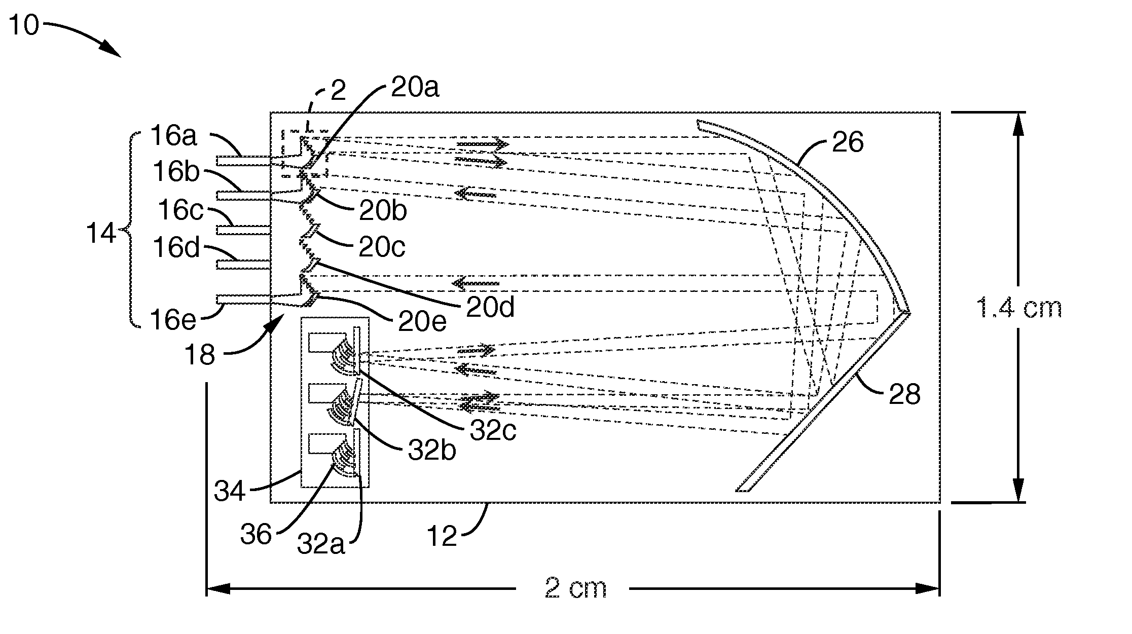
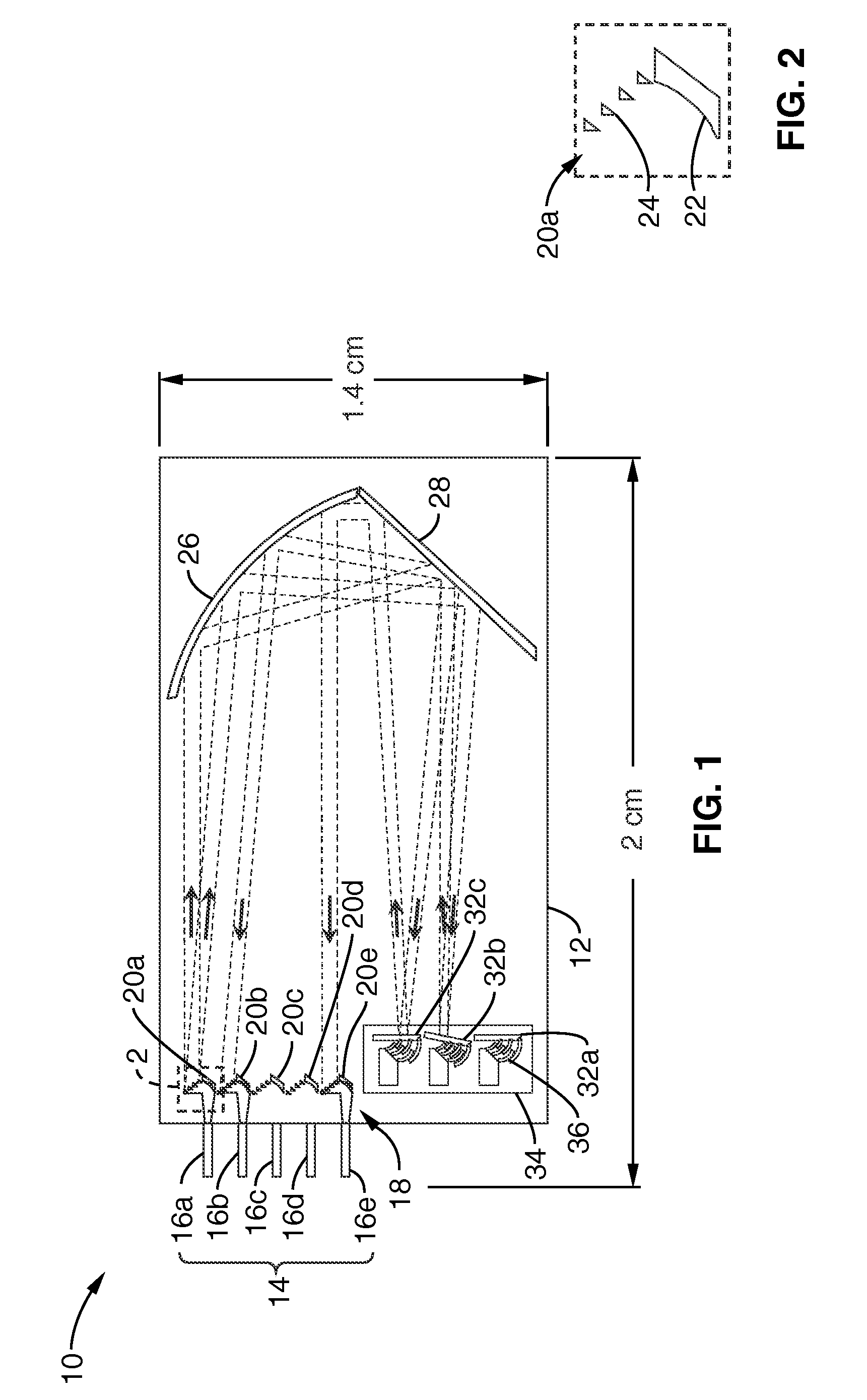
Wavelength-selective 1×N switches (WSSs) and N×N cross-connects (WSXCs) are described which are fabricated as monolithic or hybrid devices. In a preferred embodiment, the optic ports, dispersion elements, and collimating elements are formed on a single monolithic substrate. A micromirror and actuator are either fabricated within the substrate or a separate micromirror is utilized forming a hybrid WSS or WSXC. The optical elements can be formed in an opaque substrate layer (e.g., silicon, SOI, and so forth) or in an optically transparent layer of a PLC material (e.g., silica-on-silicon). Embodiments describe the use of linear and rotary comb drives for actuating front surface mirrors, or solid-immersion micromirrors (SIMs). The switching devices reduce system footprint while reducing or eliminating the need for alignment of the optical elements.

Description

CROSS-REFERENCE TO RELATED APPLICATIONS [0001] This application claims priority from U.S. provisional application serial number 60 / 741,497 filed on Dec. 1, 2005, incorporated herein by reference in its entirety.STATEMENT REGARDING FEDERALLY SPONSORED RESEARCH OR DEVELOPMENT [0002] This invention was made with Government support under DARPA Grant No. MDA972-02-1-0020. The Government has certain rights in this invention.INCORPORATION-BY-REFERENCE OF MATERIAL SUBMITTED ON A COMPACT DISC [0003] Not Applicable BACKGROUND OF THE INVENTION [0004] 1. Field of the Invention [0005] This invention pertains generally to optical switches, and more particularly to monolithic wavelength-selective switches. [0006] 2. Description of Related Art [0007] Wavelength-selective switches (WSSs) and wavelength-selective cross-connects (WSXCs) enable flexible and intelligent wavelength-division-multiplexed (WDM) networks. In addition, the use of integrated WSSs and WSXCs within networks can foster reduced op...

Claims


Application Information

Patent Timeline
Patent Type & Authority Applications(United States)
IPC IPC(8): G02B6/28G02B6/34
CPCG02B6/12021G02B6/12007
Inventor WU, MING-CHIANGCHI, CHAO-HSI
Owner RGT UNIV OF CALIFORNIA
Learn More