Epitaxial deposition of doped semiconductor materials

a semiconductor material and doped technology, applied in the direction of polycrystalline material growth, crystal growth process, chemically reactive gas, etc., can solve the problem of leaving the performance of the shallow junction device unaffected

Active Publication Date: 2007-07-12
ASM IP HLDG BV
View PDF99 Cites 34 Cited by
  • Summary
  • Abstract
  • Description
  • Claims
  • Application Information

AI Technical Summary

Benefits of technology

[0013] In another embodiment of the present invention, an apparatus for depositing semiconductor materials comprises a source of dichlorosilane vapor. The apparatus further comprises a source of (SiHzCl3-z)xCH4-x-yCly vapor, wherein 1≦x≦4, and 0≦y≦3, and (x+y)≦4, and 0≦z≦3 for each of the SiH3Cl3-z groups. The apparatus further comprises a carrier gas source. The apparatus further comprises a gas distribution network that connects the source of dichlorosilane vapor, the source of (SiHzCl3-z)xCH4-x-

Problems solved by technology

Other transistor designs benefit from elevated source/drain structures, which provide additional silicon to be consumed

Method used


Image

  • Epitaxial deposition of doped semiconductor materials
  • Epitaxial deposition of doped semiconductor materials
  • Epitaxial deposition of doped semiconductor materials

Examples


example process integration

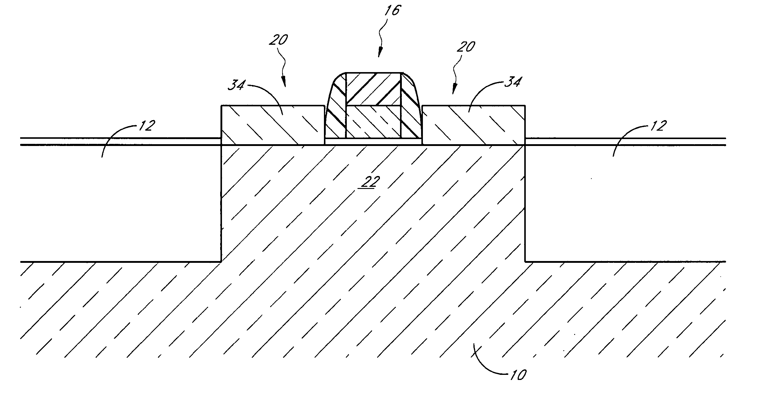
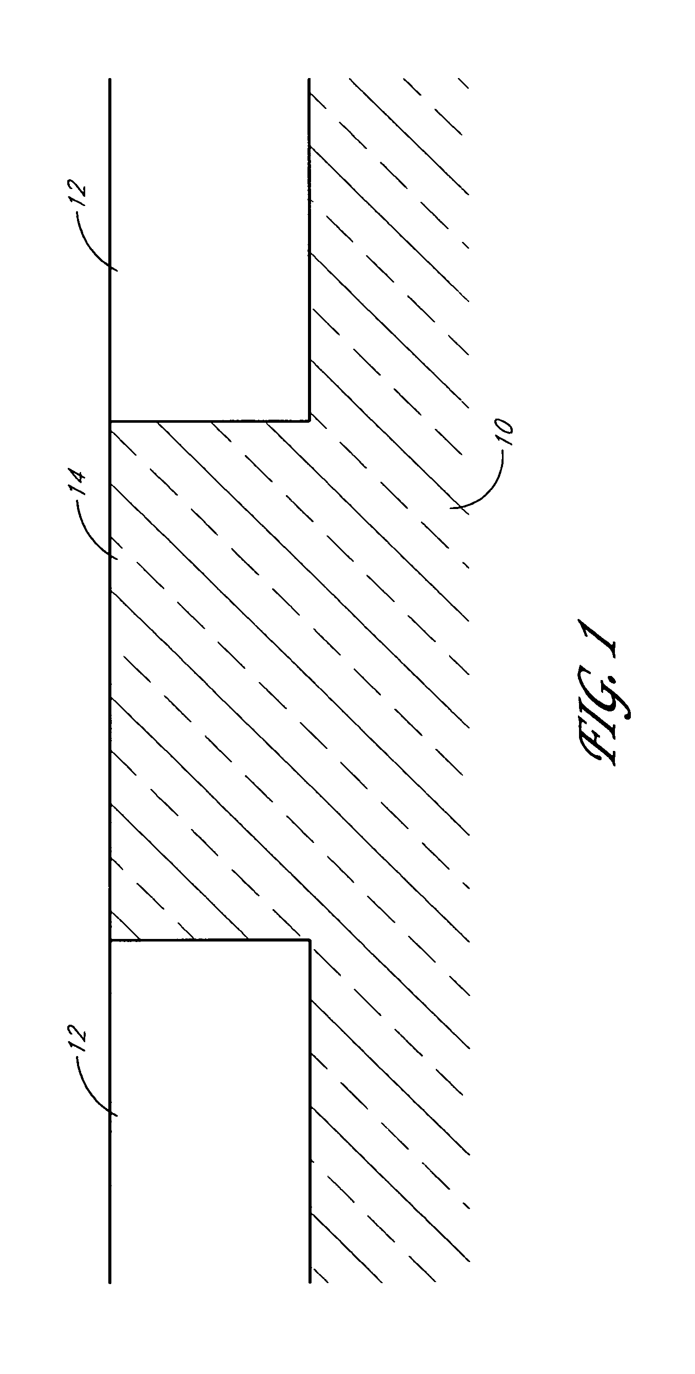
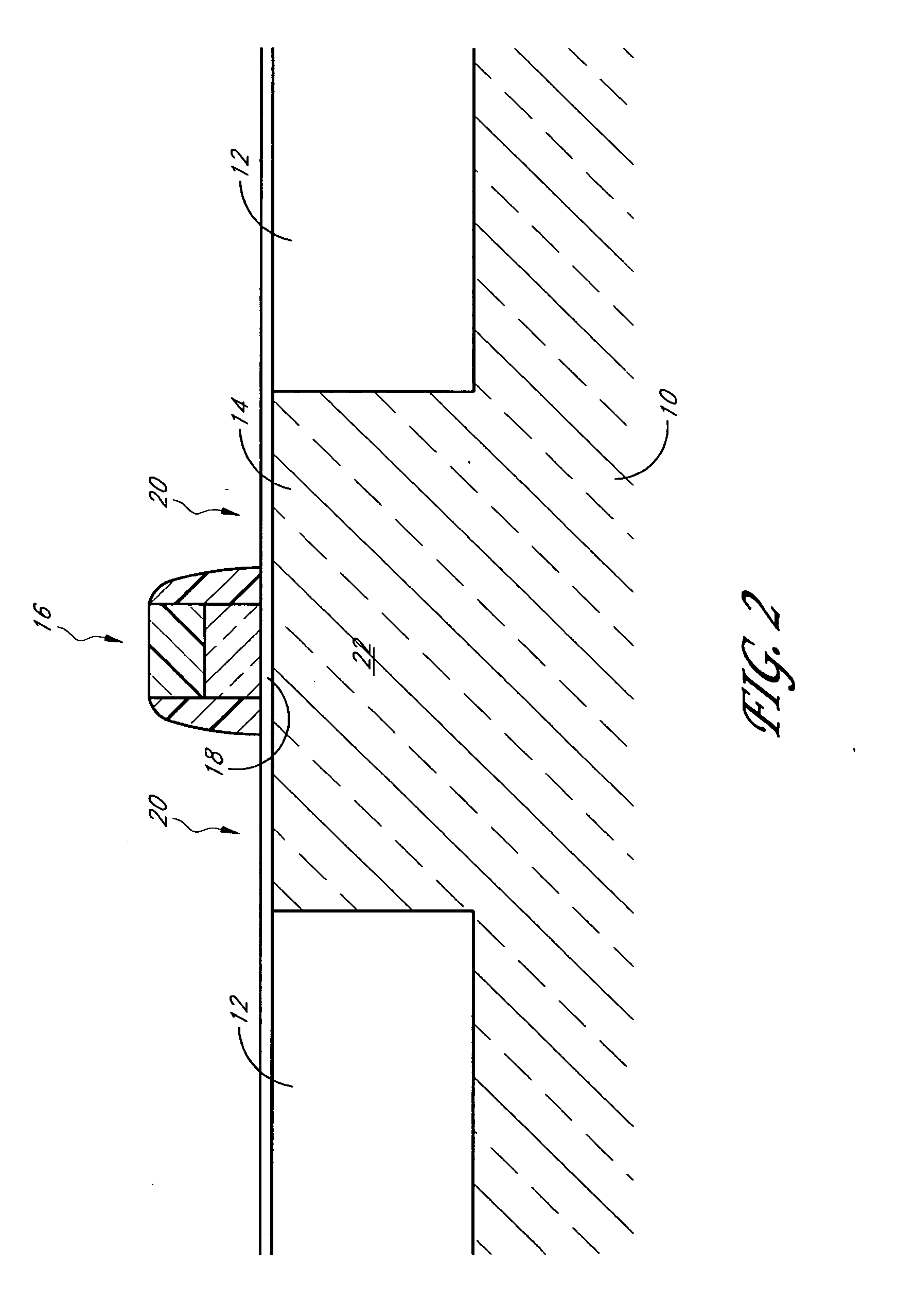
[0034]FIG. 1 illustrates a example silicon wafer substrate 10. The substrate 10 optionally includes an epitaxial layer formed over a wafer or an SOI substrate. Field isolation regions 12 have been formed by conventional shallow trench isolation (“STI”) techniques, defining active areas 14 in windows among the STI elements. Alternatively, other suitable methods are used to define field insulating material, including local oxidation of silicon (“LOCOS”) and a number of variations on LOCOS or STI. Typically, several active areas are defined simultaneously by STI across the substrate 10, and the STI often forms a web separating transistor active areas 14 from one another. In an example embodiment, the substrate is background doped at a level suitable for channel formation.

[0035]FIG. 2 illustrates the substrate 10 after formation of a gate electrode 16 over the active area 14. In the example embodiment illustrated in FIG. 2, the gate electrode 16 is illustrated as a traditional silicon ...


PUM


Abstract

A method for depositing a carbon doped epitaxial semiconductor layer comprises maintaining a pressure of greater than about 700 torr in a process chamber housing a patterned substrate having exposed single crystal material. The method further comprises providing a flow of a silicon source gas to the process chamber. The silicon source gas comprises dichlorosilane. The method further comprises providing a flow of a carbon precursor to the process chamber. The method further comprises selectively depositing the carbon doped epitaxial semiconductor layer on the exposed single crystal material.

Description

PRIORITY APPLICATIONS [0001] This application claims the benefit of U.S. Provisional Patent Application 60 / 754,569 (filed 22 Dec. 2005), the entire disclosure of which is hereby incorporated by reference herein. CROSS-REFERENCE TO RELATED APPLICATIONS [0002] This application is related to U.S. patent application Ser. No. 11 / 113,829 (filed 25 Apr. 2005; Attorney Docket ASMEX.487A); U.S. patent application Ser. No. 11 / 343,275 (filed 30 Jan. 2006; Attorney Docket ASMEX.511A); U.S. patent application Ser. No. 11 / 343,264 (filed 30 Jan. 2006; Attorney Docket ASMEX.517A); and U.S. patent application Ser. No. 11 / 343,244 (filed 30 Jan. 2006; Attorney Docket ASMEX.527A). The entire disclosure of all of these related applications is hereby incorporated by reference herein.FIELD OF THE INVENTION [0003] The present invention relates generally to epitaxial deposition, and more particularly to in situ selective epitaxial deposition of carbon-doped semiconductor materials. BACKGROUND OF THE INVENTI...

Claims


Application Information

Patent Timeline
IPC IPC(8): H01L21/20H01L21/36
CPCC30B25/02C30B29/06H01L21/0237H01L21/02381H01L21/02639H01L21/02532H01L21/02576H01L21/0262H01L21/02529H01L21/20
Inventor BAUER, MATTHIAS
Owner ASM IP HLDG BV
Why Eureka
Try Eureka