

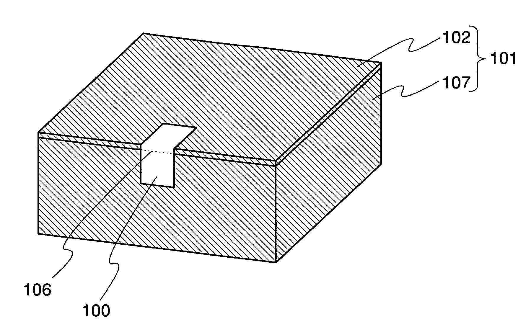
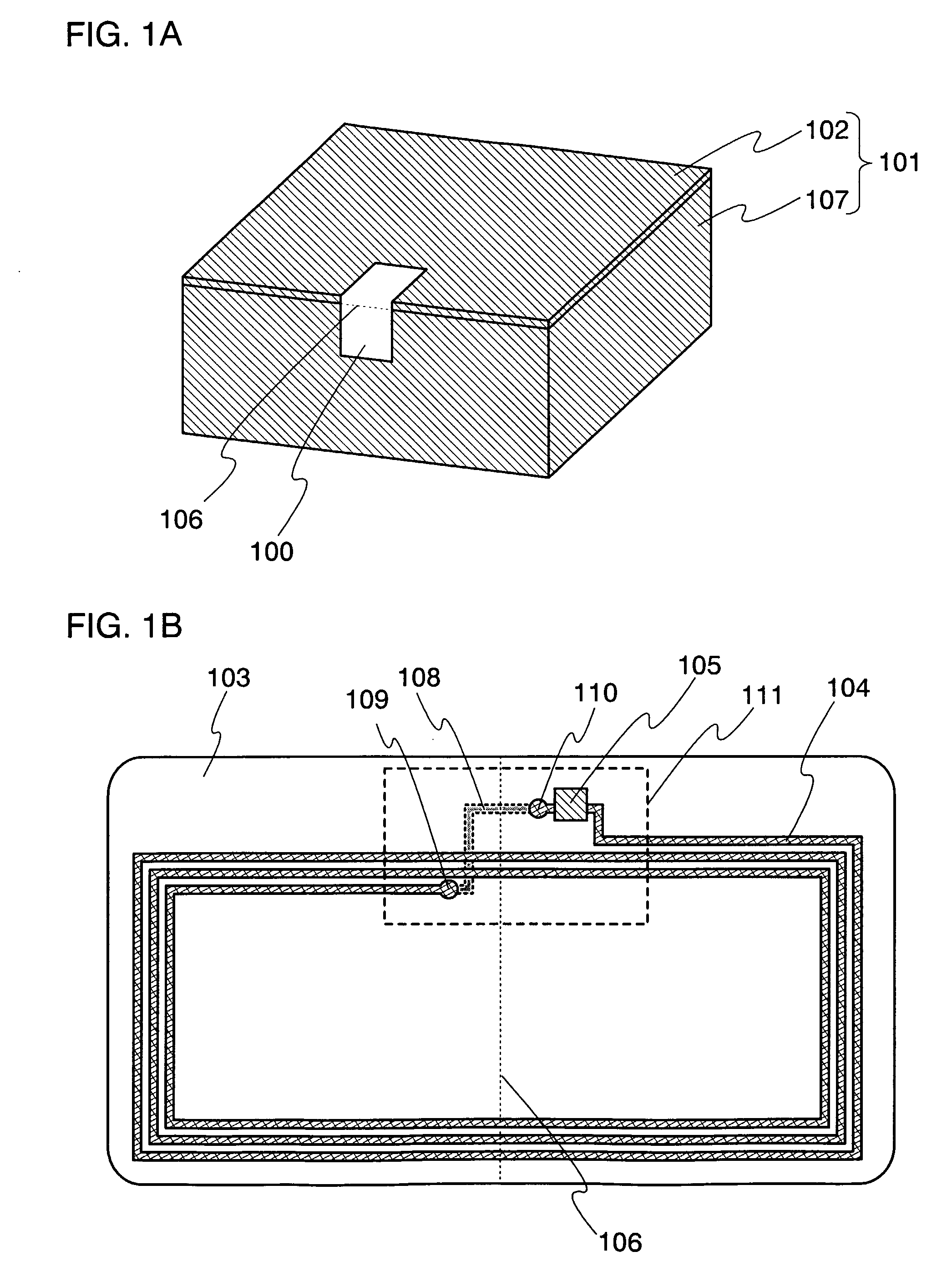
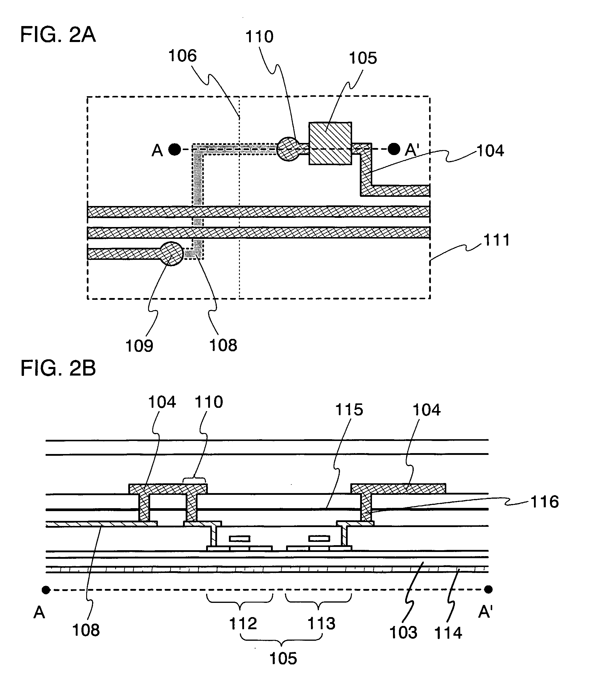
Semiconductor device
a semiconductor and device technology, applied in the field of semiconductor devices, can solve the problems of low mechanical strength of semiconductor substrates as compared to the above materials, difficult to secure circuit scale and not always cutting off antennas for sure, etc., to achieve easy to secure transmission gain of antennas, increase the application range of semiconductor devices, and high mechanical strength
- Summary
- Abstract
- Description
- Claims
- Application Information
AI Technical Summary
Benefits of technology
Problems solved by technology
Method used
Image

Examples
embodiment 1
[0100] In this embodiment, the shape of a groove is described which is formed when peeling off a plurality of integrated circuits which are formed on one substrate. FIG. 9A is a top plan view of a substrate 903 on which a groove 901 are formed. FIG. 9B is a sectional view of FIG. 9A along A-A′.
[0101] Thin film integrated circuits 902 are formed on a peeling layer 904 which is formed on the substrate 903. The groove 901 is formed between each of the thin film integrated circuits 902 and formed deep enough to expose the peeling layer 904. In this embodiment, the plurality of thin film integrated circuit 902 are not completely but partially separated by the grooves 901.
[0102] Next, FIGS. 9C and 9D show the substrates after flowing etching gas into the grooves 901 shown in FIGS. 9A and 9B to remove the peeling layer 904 by etching. FIG. 9C corresponds to a top plan view of the substrate 903 on which the grooves 901 are formed. FIG. 9D corresponds to a sectional view along A-A′ of FIG....
embodiment 2
[0105] Next, one mode of a functional structure of the semiconductor device of the invention is described with reference to FIG. 10.
[0106] Reference numeral 300 denotes an antenna and 301 denotes a thin film integrated circuit. The antenna 300 includes an antenna coil 302 and a capacitor 303 formed in the antenna coil 302. The thin film integrated circuit 301 includes a demodulating circuit 309, a modulating circuit 304, a rectifying circuit 305, a micro processor 306, a memory 307, and a switch 308 for applying a load to the antenna 300. Note that a plurality of the memory 307 may be provided as well as one.
[0107] The signals transmitted as radio waves from a reader / writer are converted into alternating electronic signals through electromagnetic induction by the antenna coil 302. The demodulating circuit 309 demodulates the alternating electronic signals and transmits them to the subsequent micro processor 306. The rectifying circuit 305 generates a power source voltage by using ...
embodiment 3
[0110] In this embodiment, an example of a semiconductor device is described in which a wiring for electrically connecting the semiconductor elements in the thin film integrated circuit passes through the separating layer. In FIG. 11A, TFTs 1101 and 1102 as one of the semiconductor elements in the thin film integrated circuit and an antenna 1103 are stuck to a support base 1104. In this embodiment, a top gate type TFT is used for the TFTs 1101 and 1102 as an example.
[0111] In FIG. 11A, a wiring which forms the antenna 1103, gate electrodes 1105 and 1106 of the TFTs 1101 and 1102 respectively are formed by patterning the same conductive film. The TFTs 1101 and 1102 are electrically connected by using a wiring 1107 which passes through a separating layer (a metal oxide film in this embodiment) 1108. In specific, the wiring 1107 and the wirings 1101 and 1111 connected to the TFTs 1110 and 1102 respectively are connected.
[0112]FIG. 11B shows the semiconductor device shown in FIG. 11A ...
PUM
 Abstract
Description
Claims
Application Information