Apparatus and methods for packaging dielectric resonator antennas with integrated circuit chips

a dielectric resonator and integrated circuit technology, applied in waveguide type devices, protection material radiating elements, basic electric elements, etc., can solve the problems of difficult manufacture and assembly of conventional waveguide front-ends, high cost and bulky wave guides, etc., to enhance antenna performance, low loss, and low dielectric constant

Inactive Publication Date: 2007-07-19
IBM CORP
View PDF5 Cites 103 Cited by
  • Summary
  • Abstract
  • Description
  • Claims
  • Application Information

AI Technical Summary

Benefits of technology

[0006] In one exemplary embodiment of the invention, an electronic package apparatus includes a package frame and an IC (integrated circuit) chip mounted to the package frame. The IC chip has an antenna feed network formed on an active surface thereof. A dielectric resonator antenna is stacked on the active surface of the ant

Problems solved by technology

For example, radio communication systems are typically built using expensive and bulky wave guides and/or package-level or board-level micro strip structures that provide electrical connections between semiconductor chips

Method used


Image

  • Apparatus and methods for packaging dielectric resonator antennas with integrated circuit chips
  • Apparatus and methods for packaging dielectric resonator antennas with integrated circuit chips
  • Apparatus and methods for packaging dielectric resonator antennas with integrated circuit chips

Examples


Embodiment Construction

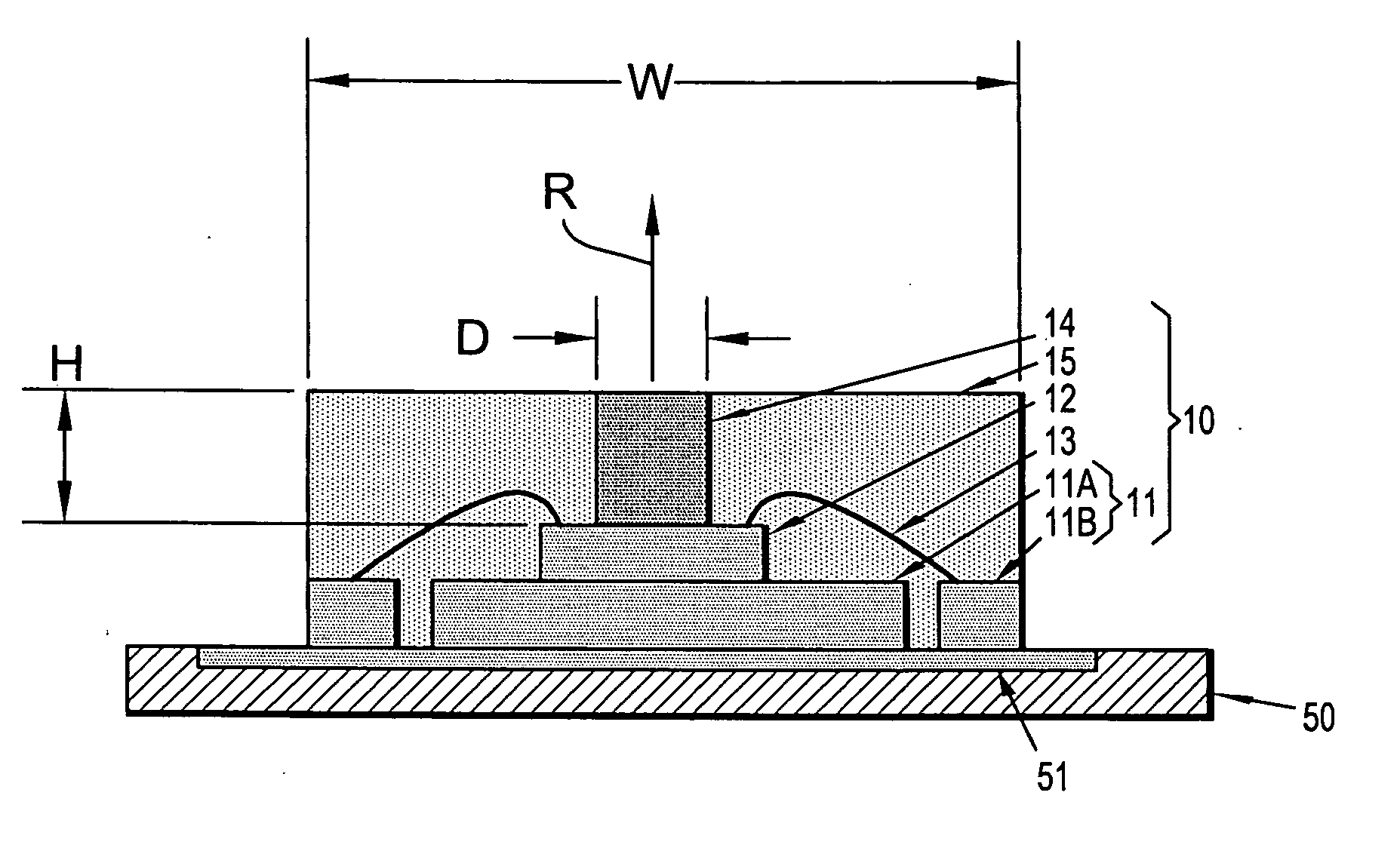
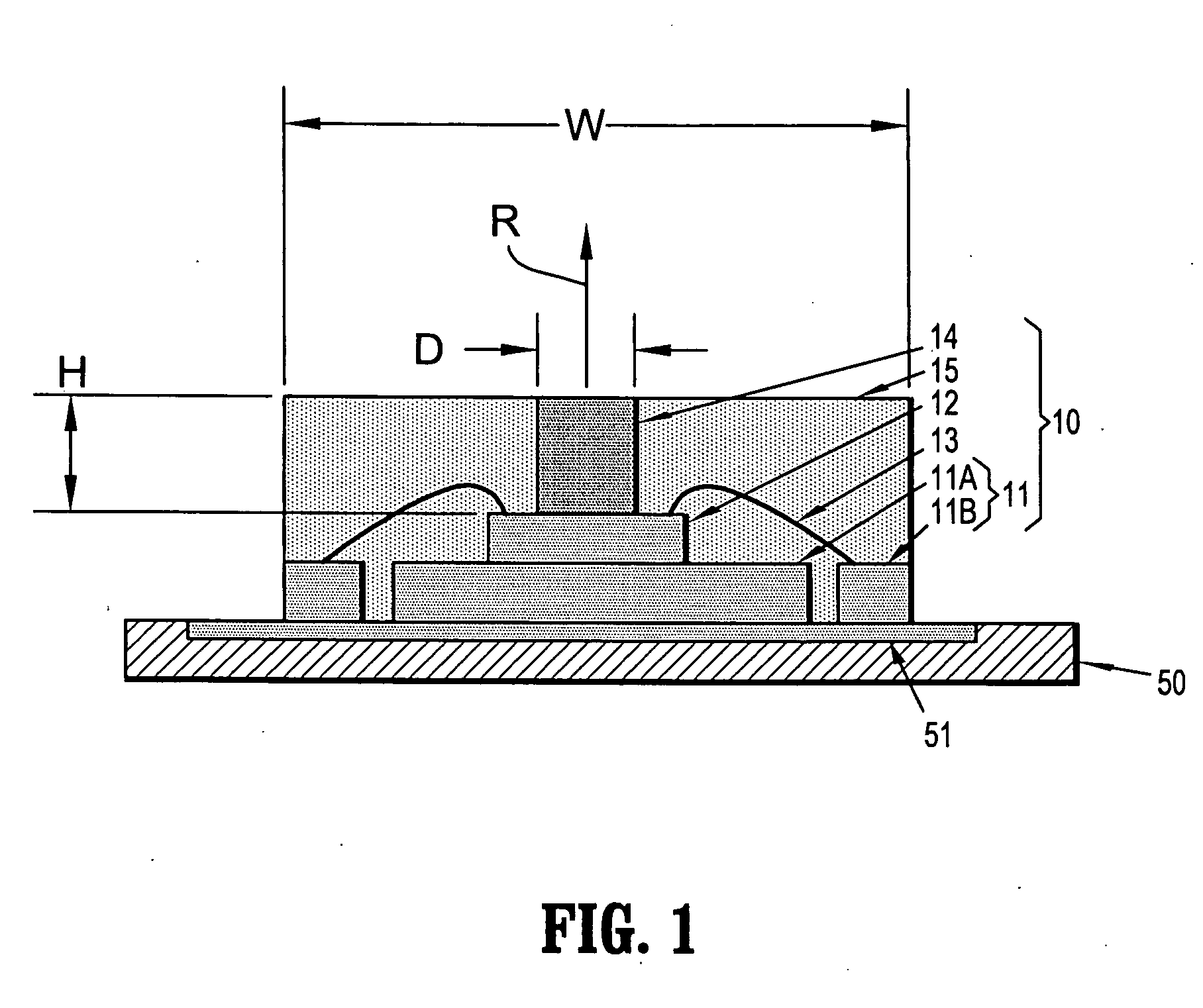
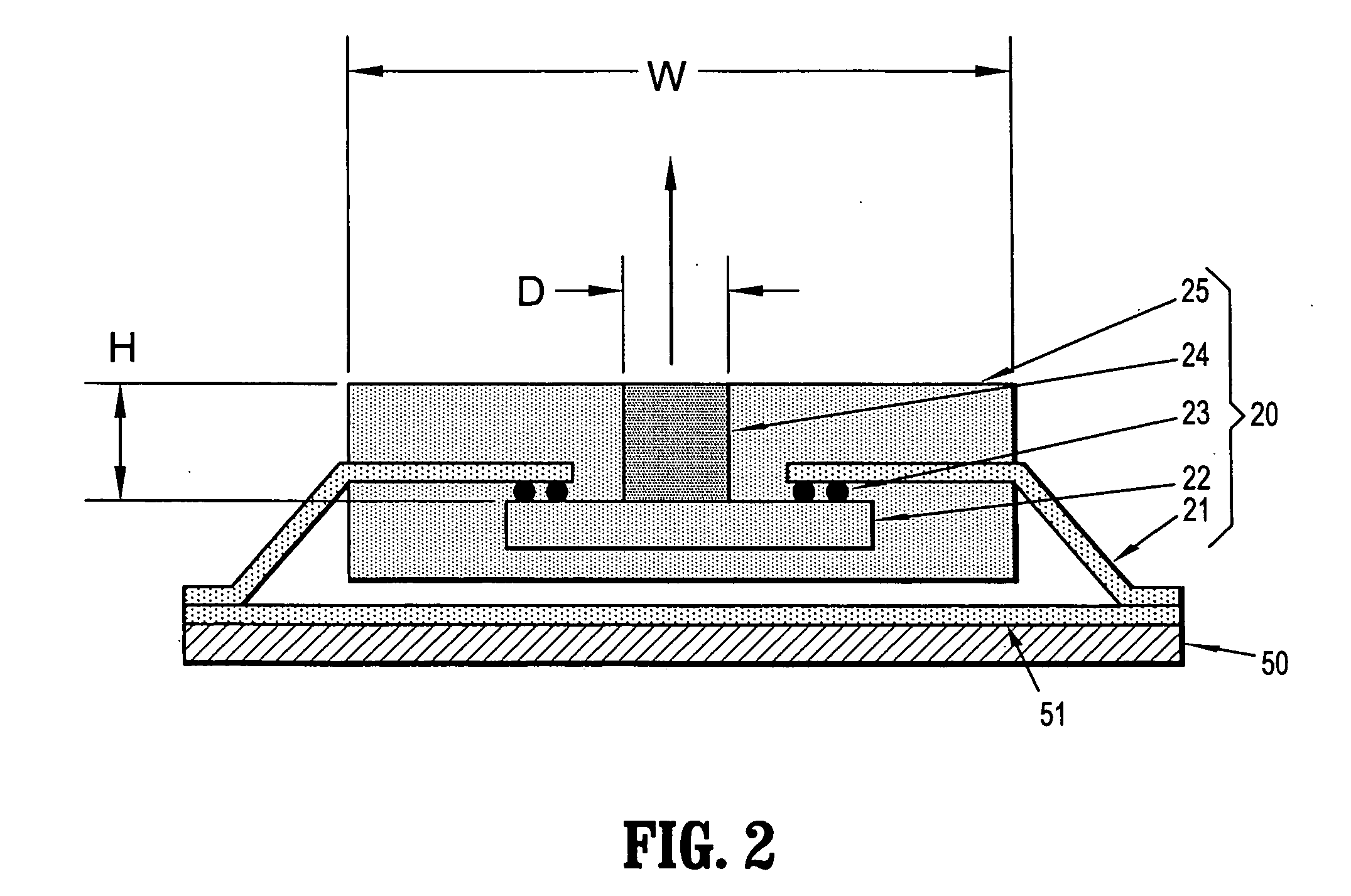
[0018] In general, exemplary embodiments of the invention as described herein include apparatus and methods for integrally packaging dielectric resonator antennas with semiconductor IC (integrated circuit) chips to provide highly-integrated and high-performance radio / wireless communications systems for millimeter wave applications (e.g., voice communication, data communication, etc.). Exemplary embodiments of the invention will be discussed with reference to FIGS. 1-5, for example, which schematically illustrate apparatus and methods for integrally packaging IC chips and dielectric resonator antennas to form compact package structures similar in size to that of existing leaded carriers or leadless chip carriers. The exemplary apparatus and methods described herein can be used to package dielectric resonator antennas together with IC chips having integrated receiver, transmitter or transceiver systems (and other RF circuits) to construct RF or wireless communications chips that opera...


PUM


Abstract

Apparatus and methods are provided for integrally packaging antenna devices with semiconductor IC (integrated circuit) chips, wherein IC chips are packaged with dielectric resonators antennas that are integrally constructed as part of a package molding (encapsulation) process, for example, to form compact integrated radio/wireless communications systems for millimeter wave applications.

Description

TECHNICAL FIELD OF THE INVENTION [0001] The present invention generally relates to apparatus and methods for integrally packaging antenna devices with semiconductor IC (integrated circuit) chips and, in particular, apparatus and methods for packaging IC chips with dielectric resonator antennas that are integrally constructed as part of a package molding (encapsulation) process, for example, to thereby form compact integrated radio / wireless communications systems for millimeter wave applications. BACKGROUND [0002] Technological innovations in wireless systems and devices have lead to widespread development of wireless network applications for wireless PAN (personal area network), wireless LAN (local area network), wireless WAN (wide area network), cellular networks, and other types of wireless communication systems. To enable wireless communication between devices in a wireless network, the devices must be equipped with receivers, transmitters, or transceivers, as well as antennas th...

Claims


Application Information

Patent Timeline
IPC IPC(8): H01L23/52
CPCH01L23/5227H01L25/16H01L2924/3025H01L2224/16245H01L2224/16225H01L2924/09701H01L2924/3011H01P7/10H01Q1/2283H01Q9/0485H01L2224/48091H01L2224/48247H01L2924/00014H01L2924/00H01L2223/6677H01L2924/15311
Inventor CHEN, ZHI NINGGAUCHER, BRIAN P.LIU, DUIXIANPFEIFFER, ULLRICH R.ZWICK, THOMAS M.
Owner IBM CORP
Why Eureka
Try Eureka